RTC – 4553AC
Page - 20
MQ - 342 - 01
Additional information
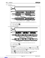
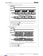
When CS0 is "L", the serial address data input at S
IN
are read at the leading edge of SCK . Next, when
WR = "H" is taken in on the 8th pulse leading edge of SCK ., the counter control register or RAM address is
selected, and data are written as shown below.
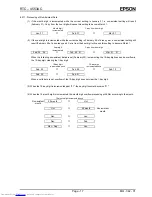
Time/calendar (CNTR = "0")
Counter data are incremented.
Example
Data before
incrementing
Number of
incrementing steps
Data after
incrementing
0
4
4
8
3
11 (10-digit is carried
automatically.)
Control register and SRAM
Address and 4-bit data are written.
The selected counter register or RAM address data are output in the following cycle from S
OUT
, in sync with the
SCK trailing edge.
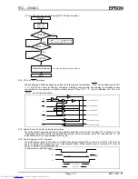
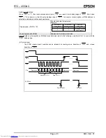
(5) System reset
The SYSR (system reset) condition can be released by causing an up transition of CS0 and a down
transition of SCK .
WR
CSo
SCK
Don't care
A0 A1 A2 A3
S
IN
System reset
Don't care
Address (1111)
D0 D1 D2 D3
Data (0111)
Don't care
SYSR bit
Release
electronic components distributor


