


RTC – 4553AC
Page - 19
MQ - 342 - 01
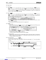
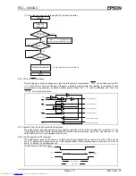
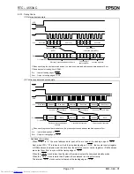
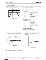
(3) Time/calendar continuous write example (CNTR=0)
Address
Access 1 (1-second digit)
Don't care
Address
Access 3 (1-minute digit)
Don't care
Address
Access 2 (10-second digit)
Don't care
Address
Data
Address
Data
Address
Data
WR
CSo
SCK
Don't care
S
IN
: Undefined
S
OUT
Previously accessed address
and data
1-second digit co 1
10-second digit co 1
⋅
The write result appears at S
OUT
when specifying the next access. When wanting to check the write result, it is
therefore necessary to specify another read or write operation. (When using write access, note that the data of
that address will be further incremented by 1.)
⋅
For continuous write operations, the CS0 must be kept "L" for the required number of increments (+1).
S
IN
: Input at leading edge of SCK
S
OUT
: Output at trailing edge of SCK
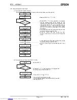
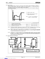
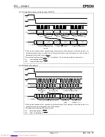
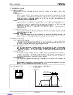
(4) SRAM data write example
d1
d2
WR
CSo
SCK
Don't care
A0
A1
A2
A3
a0
a1
a2
a3
S
IN
: Undefined
A*
A*
A*
A*
D*
D*
D*
D*
D0
D1
D2
D3
A0
A1
A2
A3
S
OUT
Previously accessed address and data
SRAM address
(0000)
Data to be written
to SRAM (1111)
SRAM address
(0000)
Next SRAM address (0001)
D0
D1
D3
D2
d0
d3
Data to be written
(1111)
⋅
The write result appears at S
OUT
when specifying the next access. When wanting to check the write result, it is
therefore necessary to specify another read or write operation.
⋅
S
IN
data are valid only during SRAM write access.
S
IN
: Input at leading edge of SCK
S
OUT
: Output at trailing edge of SCK
electronic components distributor


