

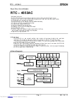


RTC – 4553AC
Page - 12
MQ - 342 - 01
8.3. How to use
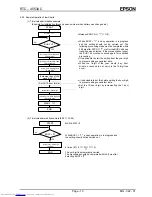
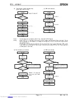
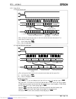
8.3.1. Data Read
When CS0 is "L", the serial address data input at S
IN
is read at the leading edge of SCK . Next, when
WR = "H" is taken in on the 8th pulse leading edge of SCK the counter control register or RAM address is
selected. The data of the selected counter control register or RAM address are output in the following cycle
from S
OUT
, in sync with the SCK trailing edge.
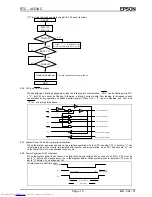
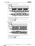
8.3.2. Data Write/Modify
When CS0 is "L", the serial address data input at S
IN
is read at the leading edge of SCK . Next, when
WR = "H" is taken in on the 8th pulse leading edge of SCK , the counter control register or RAM address is
selected, and data are written as shown below.
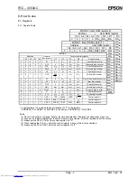
Item Content
Time/calendar
Counter, counter data increment (+1) *
Control register/RAM
Serial address/lower 4 bit of data are written
The selected counter register or RAM address data are output in the following cycle from S
OUT
, in sync
with the SCK trailing edge.
* The hour digit counter can be incremented via the 1-hour digit counter.
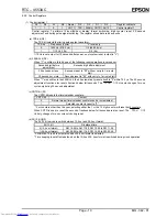
8.3.3. Initialize
(1) System reset
When the SYSR bit in the control register 3 is set to "1", all logic bits are initialized. The SYSR bit is reset to
"0" by causing an up transition of CS0 and a down transition of SCK .
Register Data
Time/calendar counters
- year, 01-month, 01-day, AM 12-hour, 00-minute,
00- second, 0-day of the week
Control registers
All "0" (SYSR = "1")
User RAM area
Undefined
Until system reset is released, TP
OUT
is fixed to "L".
1/10 Hz is not output for 10 seconds after system reset is released.
(2) Power-on-clear
At power-on, the power-on-clear function automatically performs a sequence identical to system reset.
However, because the PONC bit remains at "1", a system reset must be performed to set the PONC bit to
"0" before setting the time and calendar.
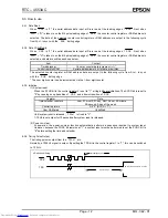
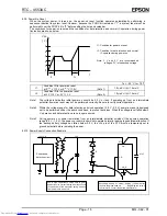
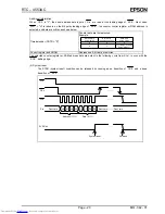
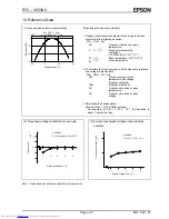
8.3.4. Timing Pulse Output
The timing pulse is output from the TP
OUT
pin.
Normally, a 1024 Hz signal is output. By setting the TPS bit in the control register 1 to "1", this can be switched
to 1/10 Hz.
•
Switchover timing
SCK
8th leading edge of SCK
TPS
Approx 60
µ
s
Switch from 1024 Hz to 1/10 Hz
electronic components distributor


