RTC – 4553AC
Page - 2
MQ - 342 - 01
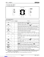
3. Terminal description
3.1. Terminal connections
RTC - 4553
1.
GND
14.
TPOUT
2.
WR
13.
S
OUT
3.
S
IN
12.
CS
1
4.
SCK
11.
CS0
5.
L
1
10.
L
5
6.
L
2
9.
L
4
7.
L
3
# 1
# 7
#14
# 8
8.
V
DD
SOP - 14 pin
3.2. Terminal functions
Signal designation
Pin No.
Input
/ Output
Function
GND
1
—
Power supply negative pin. Connect to ground.
WR
( WRITE enable )
2 I
Address and data are written at WR = "L". Counter data (second digit to
year digit) are written using the incrementing method.
Data at the specified address are read at WR = "H". While the address is
being set at S
IN
, the data at S
OUT
are for the previously specified address.
S
IN
( Serial input )
3 I
Serial address and data I/O pin. Serves for address and control register
writing for the various counters, and for RAM address and data writing.
SCK
( Serial clock )
4 I
Serial I/O sync signal input pin. Input a sync signal to this pin to allow address
and data read/write synchronized to this signal.
One cycle comprises 8 clocks (4 address 4 data clocks)
L1
−
L3
L4 , L5
5
−
7
9, 10
—
Test pins reserved for use by Epson. Be sure to leave these pins
unconnected.
V
DD
8
—
Power supply pin. Connect to a power source. For normal operation and bus
access, supply 5 V ±10% or 3 V ±10%. For backup battery operation, provide
a voltage of 2 V or higher.
See Note 1.
CS0
( Chip select 0 )
11 I
This pin serves to select the RTC. While CS0 is "L", the microprocessor
can perform register access. While CS0 is "H", S
OUT
is in the
high-impedance state.
CS1
( Chip select 1 )
12 I
Connect this pin to the power down detection circuit. If no power down
detection circuit is used, fix the pin at "H" (V
DD
). When CS1 is "L", S
OUT
and
TP
OUT
are in the high-impedance state, regardless of CS0 .
S
OUT
( Serial output )
13 O
Serial address and data output pin. Serves for address and control register
readout of the various counters, and for RAM address and data readout.
TP
OUT
( Timing pulse
output )
14 O
Output pin for 1024 Hz or 1/10 Hz timing pulse, based on internal reference
clock. For clock accuracy checking, use 1/10 Hz.
For 1024 Hz, the duty cycle changes once every 10 seconds.
Note1 At initial power-on or voltage restoration from an intermediate potential outside of the range where operation is
assured (0.3 V to 1.9 V), the power-on reset circuit may not operate normally, leading to possible malfunction.
(See section " 8.3.9. Power-On Reset ".)
Note2 Be sure to connect a bypass capacitor of 0.1
µ
F or more directly between V
DD
and GND.
electronic components distributor


