

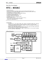


RTC – 4553AC
Page - 8
MQ - 342 - 01
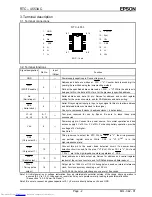
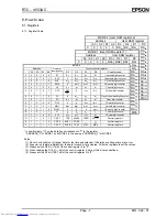
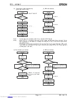
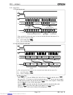
8.1.2. Register Bit Functions
Bit name
Function
Bit marked "0"
Unused bit that cannot be written. Always read as "0".
Second to year digit
BCD code. Data are written using increment method.
PM/ AM
"1" indicates PM and "0" indicates AM. This bit can be read also when 24-hour format is
selected (24/12=1). (AM: 00:00 to 11:59, PM: 12:00 to 23:59)
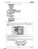
Day of the week digit
To be coded as 7-base counter.
Example
Data
0
1
2
3
4
5
6
Coded day of the week
Sun.
Mon.
Tue.
Wed.
Thu.
Fri.
Sat.
Year digit
Automatic leap year compensation up to 2099
User RAM area
30
×
4 bit SRAM
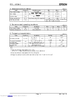
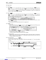
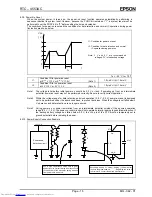
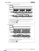
TPS
(Timing pulse selection)
Bit for selecting reference signal output
waveform.
Note 1/10 Hz is not output for 10 seconds
after power-on or system reset (output is
"L").
TPS bit
Frequency (cycle time)
0
1024 Hz (976.5
µ
s)
1
1/10 Hz (10 s)
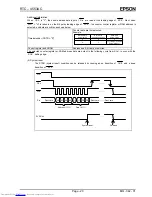
30ADJ
(30 seconds adjustment)
Setting this bit to "1" performs 30 second adjustment.
The bit automatically resets when 30 second adjustment is completed (after 76.3
µ
s).
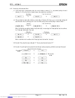
CNTR
(Counter reset)
Setting this bit to "1" resets the time and calendar counters.
24/ 12
24-hour or 12-hour format selection bit. When set to "1", 24-hour format is used. When set
to "0", 12-hour format is used.
Busy
Used when reading/writing time and calendar counter data. Set to "1" when carry occurs.
BUSY bit
Mode
Meaning
0
No carry
Time/calendar counter read/write possible
1
Carry
Time/calendar counter read/write prohibited
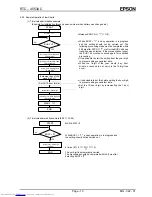
PONC
(Power-on-clear detection)
At power-on, the power-on-clear function automatically sets this bit to "1". This has the
same effect as data initialization.
Register
Data
Time/calendar counters
00- year, 01-month, 01-day, AM 12-hour,
00-minute, 00- second, 0-day of the week
Control registers
All "0" (PONC = "1")
User RAM area
Undefined
When PONC is "1", data must be set. First clear this bit (this can be done by writing "1" to
SYSR and then releasing system reset) and then set the time/calendar counters.
Bit marked "
−
"
Cannot be written. When read, the data are undefined.
Bit marked "
∗
"
Can be written but must always be set to "0".
SYSR
(System reset)
At SYSR = "1" all logic bits are initialized. The SYSR bit is reset to "0" by causing an up
transition of CS0 and a down transition of SCK.
Register
Data
Time/calendar counters
00- year, 01-month, 01-day, AM 12-hour,
00-minute, 00- second, 0-day of the week
Control registers
All "0" (SYSR = "1")
User RAM area
Undefined
TEST
Epson test bit. Must be set to "0".
MS0, MS1
(Mode selection)
These 2 bits serve for mode selection.
MS1
MS0
Mode name
Content
0
0
Mode 0
Time/calendar counters and control
registers 1 - 3
0
1
Mode 0
Time/calendar counters and control
registers 1 - 3
1
0
Mode 1
User RAM area (RA
0
- RA
59
) and control
register 3
1
1
Mode 2
User RAM area (RA
60
- RA
119
) and
control register 3
electronic components distributor


