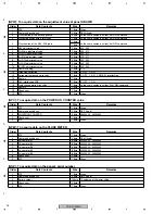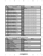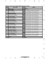
PDP-425CMX
85
5
6
7
8
5
6
7
8
C
D
F
A
B
E
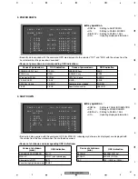
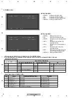
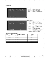
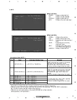
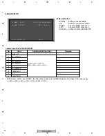
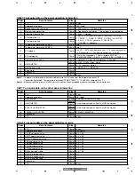
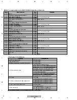
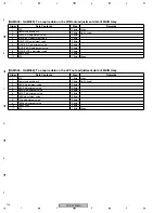
8. ETC.
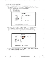
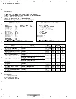
<Lower-layer items of ETC.>
• "NO OPRT" is selected when this submode is entered (to avoid accidental misoperation).
• When each item is set, the process starts then the unit shifts to the upper layer. (When NO OPRT is determined,
the unit will shift to the upper layer without doing anything.)
• When data are set to be backed up, if the digital EEPROM has not been adjusted,
do the operation of LED pattern No. 7.
A
.
P
N
T
E
C
E L
L
/
1
(
B
T
6 0 V S )
F A C T
T
E
C .
)
( +
A
.
P
N E L
L
/
1
(
B
T
6 0 V S )
F A C T
A
P R O M
B
C K U P
E E
>
< =
T
E
C .
O
: N
P R T
O
<DOWN>
: Shifting to MASK SETUP
<UP>
: Shifting to PANEL REVISE
<DISPLAY> : Shifting to MASK SETUP
<SET>
: Shifting to the next nested layer
7
Key operation
<DOWN>
: Shifting to the next item
<UP>
: Shifting to the previous item
<RIGHT>
: Adding by one to the adjustment
value
<LEFT>
: Subtracting by one from the
adjustment value
<SET>
: Determining the setting value
and shifting to the upper layer
<DISPLAY> : Shifting to MASK SETUP
7
Key operation
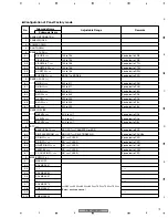
No.
Items
Adjustment/Setting Value
Remarks
1
BACKUP DATA <=>
<=>NO OPRT<=>TRANSFER<=>
"ERR" is indicated when no data are in the backup
EEPROM. To activate the option to select
TRANSFER, press the SET key about 5 seconds.
(There is a situation resting more than 5 seconds.)
2
DIGITAL EEPROM <=> <=>NO OPRT<=>REPAIR/DELETE<=>
"DELETE" is indicated when the main unit has been
already adjusted. To activate the option to select
REPAIR/DELETE, press the SET key about 5
seconds.
(There is a situation resting more than 5 seconds.)
3
PD INFO. <=>
<=>NO <=>CLEAR<=>
To activate the option to select CLEAR, repeatedly
press the SET key about 5 seconds.
(There is a situation resting more than 5 seconds.)
4
SD INFO. <=>
<=>NO <=>CLEAR<=>
5
HR-MTR INFO. <=>
<=>NO <=>CLEAR<=>
6
PM/B1-B5 <=>
<=>NO <=>CLEAR<=>
7
P COUNT INFO. <=>
<=>NO <=>CLEAR<=>
I
–
N 1
F
R
3 2 –
G B – 4
X
M
I
–
N 1
F
R
3 2 –
G B – 4
X
M
Содержание PDP-42MXE10
Страница 9: ...PDP 425CMX 9 5 6 7 8 5 6 7 8 C D F A B E ...
Страница 26: ...PDP 425CMX 26 1 2 3 4 1 2 3 4 C D F A B E 3 2 OVERALL CONNECTION DIAGRAM 2 2 Overall Wiring Diagram 2 2 ...
Страница 27: ...PDP 425CMX 27 5 6 7 8 5 6 7 8 C D F A B E ...
Страница 37: ...PDP 425CMX 37 5 6 7 8 5 6 7 8 C D F A B E ...
Страница 129: ...PDP 425CMX 129 5 6 7 8 5 6 7 8 C D F A B E ...
Страница 132: ...PDP 425CMX 132 1 2 3 4 1 2 3 4 C D F A B E MAIN PWB CONNECTOR WAVE FORM POINT SIDE B ...
Страница 133: ...PDP 425CMX 133 5 6 7 8 5 6 7 8 C D F A B E X5008 X5008 34 35 IC6304 IC6302 29 29 IC6302 29 SIDE B ...
Страница 178: ...PDP 425CMX 178 1 2 3 4 1 2 3 4 C D F A B E Pin Layout Block Diagram DS90CF388VJD MD DIGITAL ASSY IC3001 LVDS Receiver ...

