PDP-425CMX
4
1
2
3
4
1
2
3
4
C
D
F
A
B
E
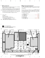
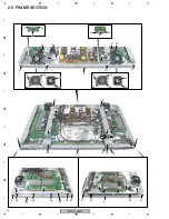
Fig.1 Charged Section and High Voltage Generating Point (Rear View)
42 SCAN B Assy
42 SCAN A Assy
SUS CLAMP 2 Assy
PLATE X (FT)
Charged Section
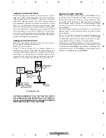
The places where the commercial AC power is used without
passing through the power supply transformer.
If the places are touched, there is a risk of electric shock. In
addition, the measuring equipment can be damaged if it is
connected to the GND of the charged section and the GND of the
non-charged section while connecting the set directly to the
commercial AC power supply. Therefore, be sure to connect the
set via an insulated transformer and supply the current.
1. Power Cord
2. AC Inlet
3. Power Switch (S1)
4. Fuse (In the POWER SUPPLY Unit)
5. STB Transformer and Converter Transformer
(In the POWER SUPPLY Unit)
6. Other primary side of the POWER SUPPLY Unit
High Voltage Generating Point
The places where voltage is 100V or more except for the charged
places described above. If the places are touched, there is a risk of
electric shock.
I f t h e p r o c e d u r e s d e s c r i b e d i n “ 7 . 1 . 4 P O W E R O N / O F F
FUNCTION FOR THE LARGE POWER SIGNAL SYSTEM”
are performed before the power is turned off, the voltage will be
discharged in about 30 seconds.
1. POWER SUPPLY Unit.....................................................(
205
V)
2. 42 X DRIVE Assy .......................................... (
–180V to 205
V)
3. 42 Y DRIVE Assy .......................................................... (
500
V)
4. 42 SCAN A Assy ............................................................ (
500
V)
5. 42 SCAN B Assy ............................................................ (
500
V)
6. SUS CLAMP 1 Assy .......................................(
–180V to 205
V)
7. SUS CLAMP 2 Assy .......................................(
–180V to 205
V)
: Part is the High Voltage Generating Points
other than the Charged Section.
: Part is Charged Section.
42 Y DRIVE Assy
42 X DRIVE Assy
SUS CLAMP 1 Assy
POWER SUPPLY Unit
Содержание PDP-42MXE10
Страница 9: ...PDP 425CMX 9 5 6 7 8 5 6 7 8 C D F A B E ...
Страница 26: ...PDP 425CMX 26 1 2 3 4 1 2 3 4 C D F A B E 3 2 OVERALL CONNECTION DIAGRAM 2 2 Overall Wiring Diagram 2 2 ...
Страница 27: ...PDP 425CMX 27 5 6 7 8 5 6 7 8 C D F A B E ...
Страница 37: ...PDP 425CMX 37 5 6 7 8 5 6 7 8 C D F A B E ...
Страница 129: ...PDP 425CMX 129 5 6 7 8 5 6 7 8 C D F A B E ...
Страница 132: ...PDP 425CMX 132 1 2 3 4 1 2 3 4 C D F A B E MAIN PWB CONNECTOR WAVE FORM POINT SIDE B ...
Страница 133: ...PDP 425CMX 133 5 6 7 8 5 6 7 8 C D F A B E X5008 X5008 34 35 IC6304 IC6302 29 29 IC6302 29 SIDE B ...
Страница 178: ...PDP 425CMX 178 1 2 3 4 1 2 3 4 C D F A B E Pin Layout Block Diagram DS90CF388VJD MD DIGITAL ASSY IC3001 LVDS Receiver ...

