PDP-425CMX
139
5
6
7
8
5
6
7
8
C
D
F
A
B
E
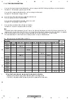
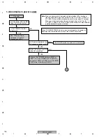
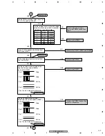
NO
YES
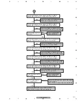
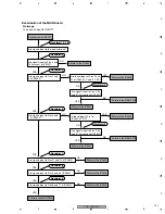
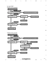
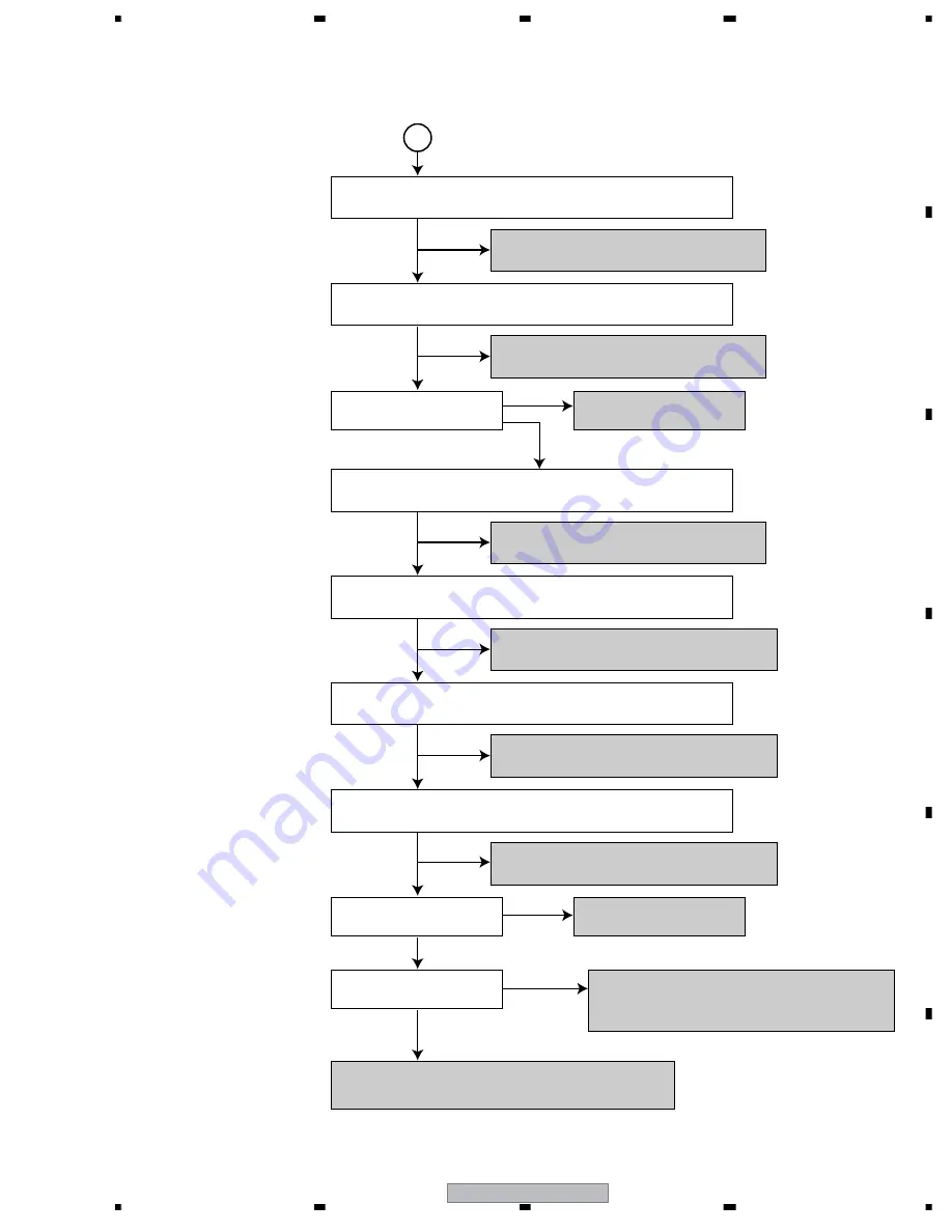
Failure in the CN2301 or LED PWB (failure in
the M5V line at Pin 8 of the CN2401)
NO
NO
YES
Failure in the COMM SLOT Assy (failure in the
M3.3V line at Pin 118 of the CN2303)
YES
Failure in the CN2302 or COMM SLOT IF PWB
(failure in the M3.3V line at Pin 16 of the CN2302)
NO
YES
NO
YES
Failure in the CN2302 or COMM SLOT IF PWB
(failure in the M5V line at Pin 20 of the CN2302)
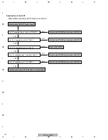
Is 5 V DC output from Pin 5
of IC9502?
Failure in the MAIN PWB
(failure in the IC9502)
NO
YES
Failure in the CN4004 or COMM SLOT IF PWB
(failure in the M3.3V line at Pin 1 of the CN4004)
Failure in the CN2201 or KEY PWB (failure in the
M3.3V line at Pin 1 of the CN9011)
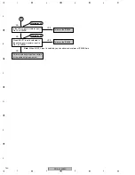
NO
YES
NO
Is 3.3 V DC output from Pin
4 of IC9503?
Failure in the MAIN PWB
(failure in the IC9503)
YES
NO (4.7V)
Is 0 V DC output from Pin
14 of CN8502 (AD2)?
YES
Failure in the MAIN PWB (failure in IC9501 or X9501)
Note: If IC9501 is in failure, replace the whole board.
Failure in the AD2 connector or MAIN PWB (failure in
IC9501 or X9501)
Note: If IC9501 is in failure, replace the whole board.
A
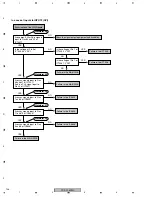
Turn the main power on with the cable to the CN2401 or CN2301
disconnected. Check if 5 V DC is output from Pin 8 of CN2301.
Turn the main power on with the cable to the CN2302 or CN9010
disconnected. Check if 5 V DC is output from Pin 20 of CN9010.
Turn the main power on with the COMM SLOT Assy disconnected from
CN2303. Check if 3.3 V DC is output from Pin 118 of CN2303.
Turn the main power on with the cable to the CN2302 or CN9010
disconnected. Check if 3.3 V DC is output from Pin 16 of CN9010.
Turn the main power on with the cable to the CN4004 or CN5301
disconnected. Check if 3.3 V DC is output from Pin 50 of CN5301.
Turn the main power on with the cable to the CN2201 or CN9011
disconnected. Check if 3.3 V DC is output from Pin 1 of CN9011.
Содержание PDP-42MXE10
Страница 9: ...PDP 425CMX 9 5 6 7 8 5 6 7 8 C D F A B E ...
Страница 26: ...PDP 425CMX 26 1 2 3 4 1 2 3 4 C D F A B E 3 2 OVERALL CONNECTION DIAGRAM 2 2 Overall Wiring Diagram 2 2 ...
Страница 27: ...PDP 425CMX 27 5 6 7 8 5 6 7 8 C D F A B E ...
Страница 37: ...PDP 425CMX 37 5 6 7 8 5 6 7 8 C D F A B E ...
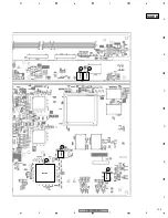
Страница 129: ...PDP 425CMX 129 5 6 7 8 5 6 7 8 C D F A B E ...
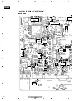
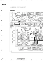
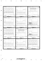
Страница 132: ...PDP 425CMX 132 1 2 3 4 1 2 3 4 C D F A B E MAIN PWB CONNECTOR WAVE FORM POINT SIDE B ...
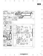
Страница 133: ...PDP 425CMX 133 5 6 7 8 5 6 7 8 C D F A B E X5008 X5008 34 35 IC6304 IC6302 29 29 IC6302 29 SIDE B ...
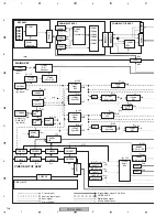
Страница 178: ...PDP 425CMX 178 1 2 3 4 1 2 3 4 C D F A B E Pin Layout Block Diagram DS90CF388VJD MD DIGITAL ASSY IC3001 LVDS Receiver ...

