PDP-425CMX
163
5
6
7
8
5
6
7
8
C
D
F
A
B
E
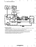
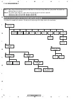
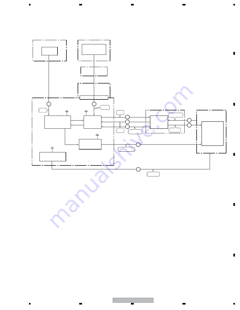
7.1.8 POWER ON SEQUENCE
Descriptions on operation
1
When the main power switch on the main unit is set to ON, M+7 V is supplied from the POWER SUPPLY Assy to the main
microcomputer to boot it.
2
A request to turn on the power is issued from a key on the main unit or remote control unit.
3
The STB_MUTE signal (STB+3.3 V, ON/OFF control) is output from the main microcomputer to the power supply.
4
STB+3.3 V is supplied from the power supply to the MD microcomputer to boot it.
5
The MD microcomputer issues the REQ_MD signal to the main microcomputer. (QS2 data read request)
6
After confirming the QS2 data read request (confirming SD or PD), the main microcomputer issues PON.
7
The MD microcomputer sends a PON echo back to the main microcomputer.
8
The MD microcomputer issues the RELAY signal to turn on the unit.
REMI
M+3.3V
KEY ASSY
MAIN ASSY
Front key
LED2 ASSY
COMM SLOT
IF ASSY
COMM SLOT
ASSY
DIGITAL ASSY
POWER SUPPLY
ASSY
Remote-control
sensor
U2401
BUFF
IC8503
Main UCOM
IC9501
MD UCOM
IC3151
Power supply
UCOM
IC3151
BUFF
Q8503,Q8504
REG
M+7V
→
M+3.3V
6
7
5
3
KEY
STB+3.3V
TXD
2
2
M+3.3V
M+3.3V
M+3.3V
RXD
REQ_MD
STB_MUTE
M+7.0V
RELAY
4
8
1
Содержание PDP-42MXE10
Страница 9: ...PDP 425CMX 9 5 6 7 8 5 6 7 8 C D F A B E ...
Страница 26: ...PDP 425CMX 26 1 2 3 4 1 2 3 4 C D F A B E 3 2 OVERALL CONNECTION DIAGRAM 2 2 Overall Wiring Diagram 2 2 ...
Страница 27: ...PDP 425CMX 27 5 6 7 8 5 6 7 8 C D F A B E ...
Страница 37: ...PDP 425CMX 37 5 6 7 8 5 6 7 8 C D F A B E ...
Страница 129: ...PDP 425CMX 129 5 6 7 8 5 6 7 8 C D F A B E ...
Страница 132: ...PDP 425CMX 132 1 2 3 4 1 2 3 4 C D F A B E MAIN PWB CONNECTOR WAVE FORM POINT SIDE B ...
Страница 133: ...PDP 425CMX 133 5 6 7 8 5 6 7 8 C D F A B E X5008 X5008 34 35 IC6304 IC6302 29 29 IC6302 29 SIDE B ...
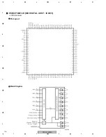
Страница 178: ...PDP 425CMX 178 1 2 3 4 1 2 3 4 C D F A B E Pin Layout Block Diagram DS90CF388VJD MD DIGITAL ASSY IC3001 LVDS Receiver ...

