PDP-425CMX
181
5
6
7
8
5
6
7
8
C
D
F
A
B
E
3
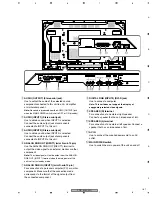
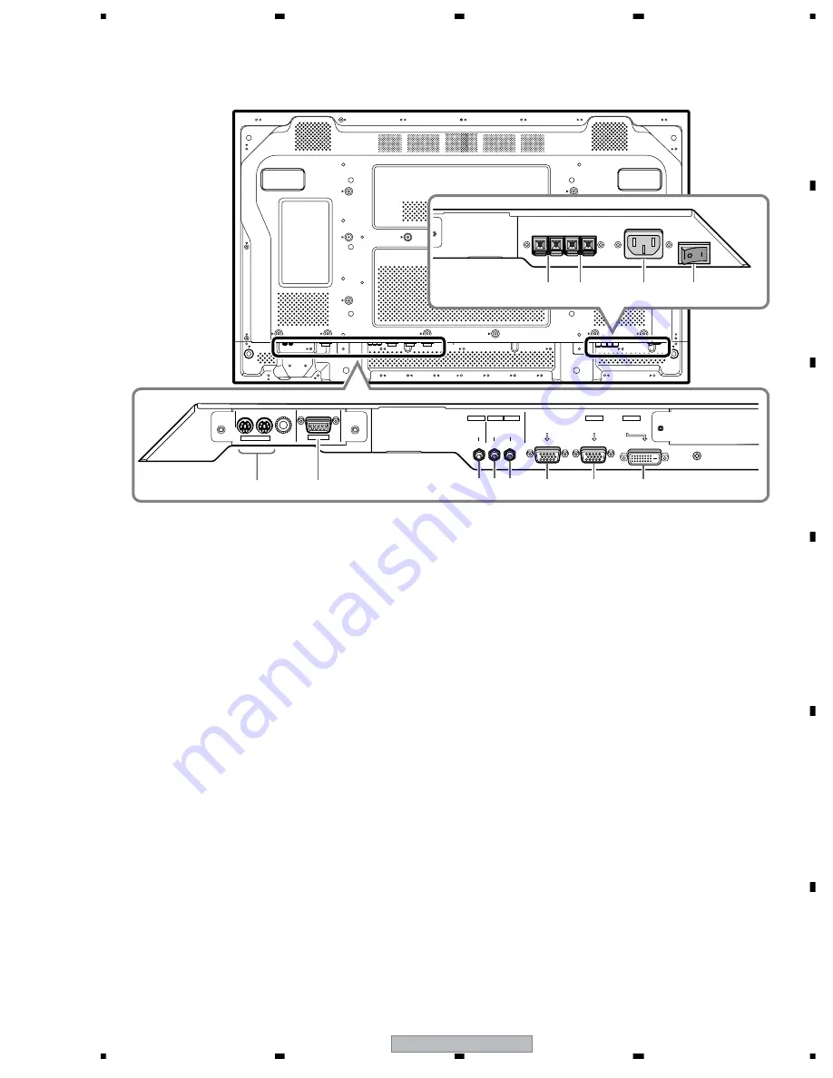
AUDIO (OUTPUT) (Stereo mini jack)
Use to output the audio of the selected source
component connected to this unit to an A V amplifier
or similar component.
Note:
No sound is produced from the AUDIO (OUTPUT) jack
when the MAIN POWER switch is set to OFF or ON (standby).
4
AUDIO (INPUT1) (Stereo mini jack)
Use to obtain sound when INPUT1 is selected.
Connect the audio output jack of components
connected to INPUT1 to this unit.
5
AUDIO (INPUT2) (Stereo mini jack)
Use to obtain sound when INPUT2 is selected.
Connect the audio output jack of components
connected to INPUT2 to this unit.
6
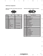
ANALOG RGB OUT (INPUT1) (mini D-sub 15 pin)
Use the ANALOG RGB OUT (INPUT1) terminal to
output the video signal to an external monitor or other
component.
Note:
The video signal will not be output from the ANALOG
RGB OUT (INPUT1) terminal when the main power of this
unit is off or in standby mode.
7
ANALOG RGB IN (INPUT1) (mini D-sub 15 pin)
For connection of a personal computer (PC) or similar
component. Make sure that the connection made
corresponds to the format of the signal output from
the connected component.
8
DIGITAL RGB (INPUT2) (DVI-D jack)
Use to connect a computer.
Note: This unit does not support the display of
copyguard-protected video signals.
9
SPEAKER (R) terminal
For connection of an external right speaker.
Connect a speaker that has an impedance of 6
Ω
.
0
SPEAKER (L) terminal
For connection of an external left speaker. Connect a
speaker that has an impedance of 6
Ω.
-
AC IN
Use to connect the supplied power cord to an AC
outlet.
=
MAIN POWER switch
Use to switch the main power of the unit on and off.
9
AUDIO AUDIO
INPUT1
AUDIO
OUTPUT
INPUT2
ANALOG RGB OUT
(D-Sub)
ANALOG RGB IN
(D-Sub)
INPUT1
DIGITAL RGB
(DVI-D)
INPUT2
IN
OUT
COMBINATION
1
RS-232C
345
6
7
8
0
-
=
2
Содержание PDP-42MXE10
Страница 9: ...PDP 425CMX 9 5 6 7 8 5 6 7 8 C D F A B E ...
Страница 26: ...PDP 425CMX 26 1 2 3 4 1 2 3 4 C D F A B E 3 2 OVERALL CONNECTION DIAGRAM 2 2 Overall Wiring Diagram 2 2 ...
Страница 27: ...PDP 425CMX 27 5 6 7 8 5 6 7 8 C D F A B E ...
Страница 37: ...PDP 425CMX 37 5 6 7 8 5 6 7 8 C D F A B E ...
Страница 129: ...PDP 425CMX 129 5 6 7 8 5 6 7 8 C D F A B E ...
Страница 132: ...PDP 425CMX 132 1 2 3 4 1 2 3 4 C D F A B E MAIN PWB CONNECTOR WAVE FORM POINT SIDE B ...
Страница 133: ...PDP 425CMX 133 5 6 7 8 5 6 7 8 C D F A B E X5008 X5008 34 35 IC6304 IC6302 29 29 IC6302 29 SIDE B ...
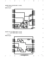
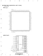
Страница 178: ...PDP 425CMX 178 1 2 3 4 1 2 3 4 C D F A B E Pin Layout Block Diagram DS90CF388VJD MD DIGITAL ASSY IC3001 LVDS Receiver ...

