PDP-425CMX
73
5
6
7
8
5
6
7
8
C
D
F
A
B
E
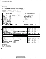
6.3 SERVICE MENU LIST
Normal
operation
MENU
MENU key
MENU key
DISPLAY 1
DISPLAY key
DISPLAY 2
DISPLAY key
Hold it pressed
for 3 sec.
INTEGRATOR
MENU
MENU key
INTEGRATOR key
MENU key
SERVICE MENU
*1 key
*1 key
*1 key: SET+CLEAR+MUTING
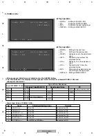
Page 1: Factory settings, frame rate conversion setting, Subscreen orbiter
setting, and PIP freeze setting
Page 2: Model name data, serial number setting/display, firmware version
display, and accumulated power-on time display
Page 3: Slot data
Page 4: Data on shutdown by the main microcomputer
For details, see "Service Menu."
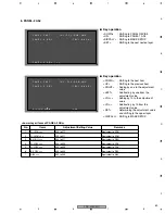
Page 8
: USAGE TIME menu (resetting USAGE TIME)
Page 9
: MONITOR INFORMATION menu
(rewriting the serial number)
Page 10 : FUNCTION menu (factory settings)
For details, see "Adjustment specifications."
Others: To be used for factory presettings
*2 key: PIP SHIFT+SET+CLEAR+PIP SHIFT or FACTORY2
For details, see "Service menu for the module."
*3 key: Left+Up+Right+POWER or FACTORY1
FACTORY MENU
*2 key
*2 key
PANEL FACTORY
MENU
*3 key
*3 key
MENU key
Three Service Factory modes are provided with this unit:
Service menu
: Mainly used for servicing. Display of shutdown data for the MAIN Assy, serial number, or accumulated power-on time
is performed. When the MAIN Assy is replaced, input the serial number, using this menu.
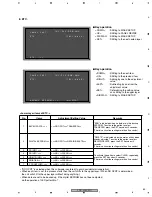
Factory menu
: Mainly used for factory presetting. The mode for line adjustment is displayed. Not for normal use.
When the MAIN Assy is replaced, factory shipment setting (P69) is required.
For details, see "Adjustment after the replacement of MAIN Assy" (6.2 ADJUSTMENT).
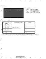
Panel Factory menu
: Mainly used for servicing. Display of power-down data inside the module and of accumulated power-on time,
MASK ON/OFF, and setting of the Vofs voltage can be performed. When either the MD DIGITAL Assy,
Service panel, or power supply unit is replaced, setting is required, using this menu. For details, see
"6.7 METHOD FOR REPLACING THE SERVICE PANEL ASSY", "7.1.5 BACKUP WHEN THE MAIN
UNIT IS ADJUSTED".
Содержание PDP-42MXE10
Страница 9: ...PDP 425CMX 9 5 6 7 8 5 6 7 8 C D F A B E ...
Страница 26: ...PDP 425CMX 26 1 2 3 4 1 2 3 4 C D F A B E 3 2 OVERALL CONNECTION DIAGRAM 2 2 Overall Wiring Diagram 2 2 ...
Страница 27: ...PDP 425CMX 27 5 6 7 8 5 6 7 8 C D F A B E ...
Страница 37: ...PDP 425CMX 37 5 6 7 8 5 6 7 8 C D F A B E ...
Страница 129: ...PDP 425CMX 129 5 6 7 8 5 6 7 8 C D F A B E ...
Страница 132: ...PDP 425CMX 132 1 2 3 4 1 2 3 4 C D F A B E MAIN PWB CONNECTOR WAVE FORM POINT SIDE B ...
Страница 133: ...PDP 425CMX 133 5 6 7 8 5 6 7 8 C D F A B E X5008 X5008 34 35 IC6304 IC6302 29 29 IC6302 29 SIDE B ...
Страница 178: ...PDP 425CMX 178 1 2 3 4 1 2 3 4 C D F A B E Pin Layout Block Diagram DS90CF388VJD MD DIGITAL ASSY IC3001 LVDS Receiver ...


