PDP-425CMX
82
1
2
3
4
1
2
3
4
C
D
F
A
B
E
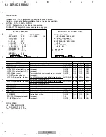
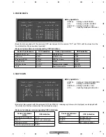
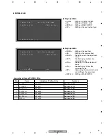
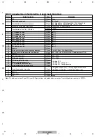
5. PANEL-1 ADJ
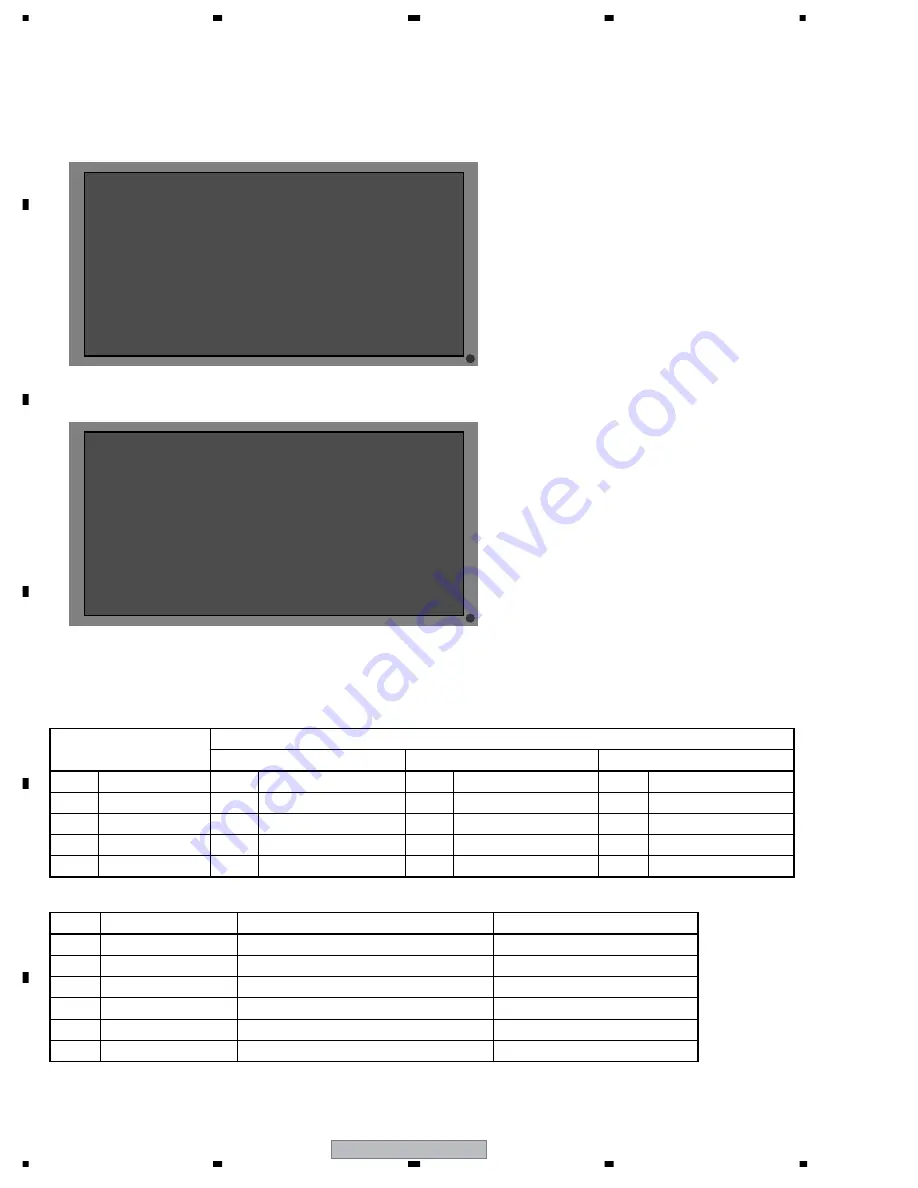
<Drive-sequence indications and indications for the ABL/WB tables>
(The OSD indications are displayed at the right part of the third line for submode PANEL-1 ADJ and
subsequent submodes.)
<Lower-layer items of PANEL-1 ADJ>
A
.
P
N E L
L
/
1
(
B
T
6 0 V S )
F A C T
A
J
P
N E L – 1
A D
<DOWN>
: Shifting to the next item
<UP>
: Shifting to the previous item
<RIGHT>
: Adding by one to the adjustment
value
<LEFT>
: Subtracting by one from the
adjustment value
<VOL+>
: Adding by 10 to the adjustment
value
<VOL->
: Subtracting by 10 from the
adjustment value
<SET>
: Determining the adjustment value
and shifting to the upper layer
<DISPALY> : Shifting to MASK SETUP
A
.
P
N E L
L
/
1
(
B
T
6 0 V S )
F A C T
–
X
S U S – B
A
J
P
N E L – 1
A D
2
: 1
8
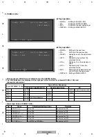
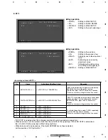
Type of WB/ABL Tables
Type of Drive Sequences
Standard Video/MASK ON
Nonstandard Video
PC
TBL1
48VS
---
60PS
Not used for consumer products
TBL2
50VS
50VN
70PS
TBL3
60VS
60VN
TBL4
72VS
Only Mask indication
---
75VS
75VN
No.
Items
Adjustment/Setting Value
Remarks
1
X-SUS B <=>
120 to 136
Equivalent to XSB
2
Y-SUS B <=>
120 to 136
Equivalent to YSB
3
Y-SUSTAIL T <=>
120 to 136
Equivalent to YTG
4
Y-SUSTAIL W <=>
120 to 136
Equivalent to YTW
5
6
XY-RST W <=>
120 to 136
Equivalent to RSW
SUS FREQ. <=>
<=>MODE1 to MODE8<=>
Equivalent to SFR
<DOWN>
: Shifting to PANEL-2 ADJ
<UP>
: Shifting to POWER DOWN
<SET>
: Shifting to the next nested layer
<DISPLAY> : Shifting to MASK SETUP
7
Key operation
7
Key operation
+
2 3
2 3
5
∞
I
–
N 1
F
R
3 2 –
G B – 4
X
M
I
–
N 1
F
R
3 2 –
G B – 4
X
M
Содержание PDP-42MXE10
Страница 9: ...PDP 425CMX 9 5 6 7 8 5 6 7 8 C D F A B E ...
Страница 26: ...PDP 425CMX 26 1 2 3 4 1 2 3 4 C D F A B E 3 2 OVERALL CONNECTION DIAGRAM 2 2 Overall Wiring Diagram 2 2 ...
Страница 27: ...PDP 425CMX 27 5 6 7 8 5 6 7 8 C D F A B E ...
Страница 37: ...PDP 425CMX 37 5 6 7 8 5 6 7 8 C D F A B E ...
Страница 129: ...PDP 425CMX 129 5 6 7 8 5 6 7 8 C D F A B E ...
Страница 132: ...PDP 425CMX 132 1 2 3 4 1 2 3 4 C D F A B E MAIN PWB CONNECTOR WAVE FORM POINT SIDE B ...
Страница 133: ...PDP 425CMX 133 5 6 7 8 5 6 7 8 C D F A B E X5008 X5008 34 35 IC6304 IC6302 29 29 IC6302 29 SIDE B ...
Страница 178: ...PDP 425CMX 178 1 2 3 4 1 2 3 4 C D F A B E Pin Layout Block Diagram DS90CF388VJD MD DIGITAL ASSY IC3001 LVDS Receiver ...

