PDP-425CMX
144
1
2
3
4
1
2
3
4
C
D
F
A
B
E
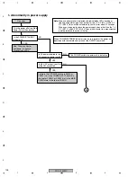
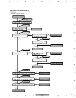
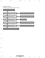
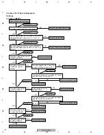
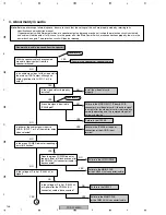
Examination of the SLOT input
Failure in the MAIN PWB
Failure in the MAIN PWB
Failure in the MAIN PWB
Failure in the IF PWB
Are signals input to the SLOT input section?
NO
NO
Failure in the harness ADX3274
NO
YES
YES
Are sync signals input to Pins 15 and 19 of CN4005?
And are video signals input to Pins 3, 7 and 11 of
CN4005?
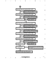
Are sync signals input to Pins 1 and 5 of CN5001?
And are video signals input to Pins 9, 13 and 17 of
CN5001?
NO
YES
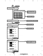
Are signals input to Pins 4 and 10
(for sync) of IC5001?
NO
NO
YES
Are signals input to Pins 2, 4 and 30 (for control)
and Pin 31 (3.3V DC) of IC5902?
Are signals input to Pins 2, 4 and 30 (for control)
and Pin 31 (3.3V DC) of IC5301?
NO
YES
NO
YES
YES
NO
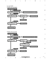
Are signals input to Pins
11 and 13 of IC5903?
Failure in the IC9504
Failure in the IC5903
Failure in the IC5301
Failure in the IC5301
Failure in the IC5001
Failure in the IC5904
Failure in the IC5902
NO
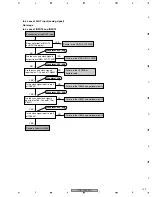
Are signals input to Pins
3 and 6 of IC9504?
YES
YES
YES
Are signals input to Pins
7 and 9 (for sync) of
IC5902?
Are the voltages at Pins 2 and 14 (for
control) of IC5902 0V and 5V DC?
YES
NO
YES
NO
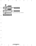
Are signals input to Pins
4 and 7 of IC5904?
Is the voltage at Pin 1 of
IC5904 0V DC?
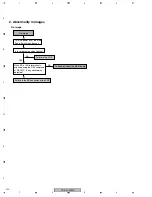
No image
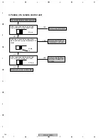
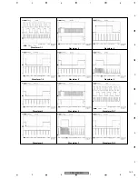
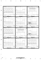
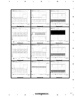
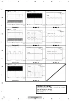
In a case of INPUT5
In a case of SLOT input (analog signal)
Waveform 17
Waveform 15
Waveform 19
Waveform 18
Waveform 16
Waveform 14
Waveform 13
Waveform 12-1, 12-2
Waveform 11-1, 11-2
Waveform 10-1, 10-2
Failure in the VIDEO SLOT PWB
Содержание PDP-42MXE10
Страница 9: ...PDP 425CMX 9 5 6 7 8 5 6 7 8 C D F A B E ...
Страница 26: ...PDP 425CMX 26 1 2 3 4 1 2 3 4 C D F A B E 3 2 OVERALL CONNECTION DIAGRAM 2 2 Overall Wiring Diagram 2 2 ...
Страница 27: ...PDP 425CMX 27 5 6 7 8 5 6 7 8 C D F A B E ...
Страница 37: ...PDP 425CMX 37 5 6 7 8 5 6 7 8 C D F A B E ...
Страница 129: ...PDP 425CMX 129 5 6 7 8 5 6 7 8 C D F A B E ...
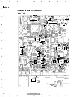
Страница 132: ...PDP 425CMX 132 1 2 3 4 1 2 3 4 C D F A B E MAIN PWB CONNECTOR WAVE FORM POINT SIDE B ...
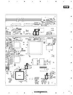
Страница 133: ...PDP 425CMX 133 5 6 7 8 5 6 7 8 C D F A B E X5008 X5008 34 35 IC6304 IC6302 29 29 IC6302 29 SIDE B ...
Страница 178: ...PDP 425CMX 178 1 2 3 4 1 2 3 4 C D F A B E Pin Layout Block Diagram DS90CF388VJD MD DIGITAL ASSY IC3001 LVDS Receiver ...

