1
ORTEC MODEL 572A
SPECTROSCOPY PILE-UP AMPLIFIER
1. DESCRIPTION
1.1. GENERAL
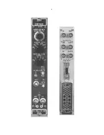
The ORTEC 572A Spectroscopy Amplifier and
Pile-Up Rejector is a single-width NIM module with
a versatile combination of switch-selectable pulse-
shaping and output characteristics. It features
extremelylownoise,widegainrange,andexcellent
overloadresponseforuniversal application inhigh-
resolution spectroscopy. It accepts input pulses of
either polarity that originate in germanium or silicon
semiconductor detectors, in scintillation counters
with either fast or slow scintillators, in proportional
counters,inpulsedionizationchambers,inelectron
multipliers, etc.
The572Ahasaninputimpedanceofapproximately
500Ω and accepts either positive or negative input
pulses with rise times <650 ns and fall times >40
µs. Six integrate and differentiate time constants
are switch-selectable to provide optimum shaping
forresolutionandcountrate.Thefirstdifferentiation
network has variable pole-zero cancellation that
can be adjusted to match preamplifiers with decay
times>40µs.Thepole-zerocancellationdrastically
reduces the undershoot after the first differentiator
and greatly improves overload and count rate
characteristics. In addition, the amplifier contains
an active filter shaping network that optimizes the
signal-to-noise ratio and minimizes the overall
resolving time. Both unipolar and bipolar outputs
are provided simultaneously on the front and rear
panels.
The unipolar output should be used for
spectroscopy when dc coupling can be maintained
from the 572A to the analyzer. A BLR (baseline
restorer)circuitisincludedinthe572Aforimproved
performance at all count rates. Baseline correction
is applied during intervals between input pulses
onlyandafrontpanelswitchselectsadiscriminator
level to identify input pulses. The unipolar output dc
level can be adjusted in the range from -100 mV to
+100 mV. This output permits the use of the direct-
coupled input of the analyzer with a minimum
amount of interface problems. The 572A bipolar
output may be preferable for spectroscopy when
operating into an ac-coupled system at high
counting rates.
Internal pulse pileup (a second pulse arriving
before the first pulse has been completed) is
sensed internally. The 572A includes an Inhibit
output BNC connector on therearpanelthatcan be
used to inhibit measurement of the result of a pulse
pileup when it occurs.
The 572A can be used for constant-fraction timing
when operated in conjunction with an ORTEC 551
or 552 Timing Single-Channel Analyzer. The
ORTEC timing single-channel analyzers feature a
minimum of walk as a function of pulse amplitude
and incorporate a variable delay time on the output
pulse to enable the timing pickoff output to be
placed in time coincidence with other signals.
The 572A has complete provisions, including
power, for operating any ORTEC solid-state
preamplifier. Normally, the preamplifier pulses
should have a rise time of 0.25 µs or less to
properly match the amplifier filter network and a
decay time greater than 40 µs for proper pole-zero
cancellation. The 572A input impedance is 500Ω.
Whenlongpreamplifiercablesareused,thecables
can be terminated in series at the preamplifier end
or in shunt at the amplifier end with the proper
resistors. The output impedance is about 0.1Ω at
the front panel connectors and 93Ω at the rear
panel connectors. The front panel outputs can be
connected to other equipment by a single cable
going to all equipment and shunt terminated at the
far end of the cabling. If series termination is
desired, the rear panel connectors can be used to
connect the 572A to other modules. See Section 3
for further information.
1.2. POLE-ZERO CANCELLATION
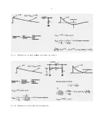
Pole-zero cancellation is a method for eliminating
pulse undershoot after the first differentiating
network. In an amplifier not using pole-zero
cancellation (Fig. 1.1), the exponential tail on the
preamplifier output signal (usually 50 to 500 µs)
Содержание 572A
Страница 6: ...vi...
Страница 24: ...18 Fig 4 16 Gamma Ray Charged Particle Coincidence Experiment Fig 4 17 Gamma Ray Pair Spectrometry...
Страница 26: ...20 Fig 5 1 Amplifier Block Diagram...


