9
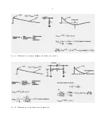
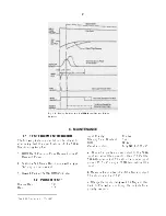
Fig. 4.1. Typical Effects of Shaping-Time Selection on
Output Waveforms.
any level from X1.0 through X1500, using all three
of these controls.
POS/NEG
A toggle switch selects an input circuit
that accepts either polarity of pulses from the
preamplifier.
PZ ADJ
A screwdriver control to set the pole-zero
cancellation to match the preamplifier pulse decay
characteristics. The range is from 40 µs to infinity.
DC
A screwdriver control adjusts the dc baseline
level of the unipolar output in the range of -0.1 V to
+0.1 V.
SHAPING
A 6-position switch selects equal
integrate and differentiate time constants to shape
the input pulses. Settings are 0.5, 1, 2, 3, 6, and
10 µs.
BLR
A 3-position toggle switch controls the
operation of the internal baseline restorer (BLR)
circuit. The center setting of the switch is effectively
Off, and this permits adjustment of the PZ Adj
control without interference from the BLR circuit.
The Auto setting of the switch selects a circuit that
regulates the threshold of the BLR gate according
to the output noise level. The Threshold setting
permits manual control of the BLR gate threshold
usingthescrewdrivercontrolimmediatelybelowthe
toggle switch.
4.3. FRONT PANEL CONNECTORS
INPUT
Accepts input pulses to be shaped and/or
amplified by the 572A. Compatible characteristics;
positive or negative with rise time from 10 to 650
ns; decay time greater than 40 µs for proper pole-
zero cancellation; input linear amplitude range 0 to
10 V, with a maximum limit of ±20 V. Input
impedance is approximately 500Ω.
UNI
Provides a unipolar positive output with
characteristics that are related to input peak
amplitude, gain, shaping time constants, pole-zero
cancellation, and baseline stabilization. The dc
baseline level is adjustable for offset to ±0.1 V.
Output impedance through this connector is about
0.1 Ω, dc coupled. Linear range 0 to +10V.
BI
Provides a bipolar pulse with positive lobe
leading and with characteristics that are related to
input peak amplitude, gain, and shaping time
constants. Timing is prompt with respect to the
input. Crossover walk of this output is less than 3
ns (see Specifications). Output impedance through
Содержание 572A
Страница 6: ...vi...
Страница 24: ...18 Fig 4 16 Gamma Ray Charged Particle Coincidence Experiment Fig 4 17 Gamma Ray Pair Spectrometry...
Страница 26: ...20 Fig 5 1 Amplifier Block Diagram...


