19
Fig. 4.18. Gamma-Gamma Coincidence Experiment.
5. CIRCUIT DESCRIPTION
Figure 5.1 is a block diagram of the instrument.
Much of the circuitry in the 572A has been
designed to use ORTEC Hybrid circuits. This
advanced technology achieves an economical
high-density package with high reliability.
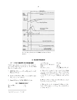
Figure 5.2 illustrates the relative timing of the
signalsinthe572A. The solid-linewaveformsshow
a normal response to a single linear input signal
from the preamplifier without any pulse pileup. The
broken-line waveforms show the modifications that
occur when there is a pileup condition.
The input from the preamplifier is a step change
with a very long decay and this is repeated and
differentiated at test point TP3. The 572A output
that results from this input is shaped, rising to its
peak in 2τ, where τ is the selected time constant of
0.5, 1, 2, 3, 6, or 10 µs. The amplifier produces the
fast shaped pulse from the same preamplifier input
pulse, and this triggers discriminator IC12, set just
above the noise level. The discriminator response
triggers the CRM output signal. The discriminator
response also triggers the Busy output signal,
which has a duration of 6τ, equal to the duration of
the linear output signal. The Inhibit output remains
low in the absence of a second pulse from the
preamplifier.
Using the broken-line waveforms to show the
variations when there is a pulse pileup, the second
pulse arrives before the Busy output signal
recovers.Thelinearoutputsignalisdistortedbythe
second pulse. The fast amplifier generates another
output that again triggers the discriminator to
produce another CRM output pulse and to update
the Busy output. Since the bistable for the Inhibit
output has been set by the first pulse, the Inhibit
output is generated, starting at the response to the
secondpulseandextendingthroughthe6τupdated
interval of the Busy output.
Содержание 572A
Страница 6: ...vi...
Страница 24: ...18 Fig 4 16 Gamma Ray Charged Particle Coincidence Experiment Fig 4 17 Gamma Ray Pair Spectrometry...
Страница 26: ...20 Fig 5 1 Amplifier Block Diagram...


