UNC/WN5/FN5/DN5
40838301TH Rev.1
A3 - 40
4.3
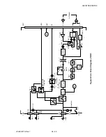
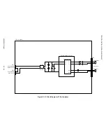
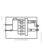
FN5 circuit diagram
1
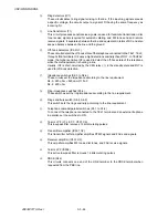
Lightning arresters (AR1, 2)
The nominal operating voltage is 500 V.
When connecting the ground of the arrestor to the chassis, tighten ARG on the PCB
with a screw. At this time, the PCB is grounded through the power cable.
The TB1 arrestor ground terminal can also be used to connect to the earth directly.
3
Diode bridge (DB1)
This circuit rectifies the loop current so that the DC circuit characteristics are not
affected by a polarity change over the line.
4
DC circuits (Q3, R540, R541, C13, R9, R209)
These circuits provide DC characteristics according to the line requirements.
5
Impedance matching network (R523, R536, C503, R623, R636, C603)
This circuit matches the impedance between the line and equipment to reduce
reflection of transmitted signals.
It provides impedance (return loss) characteristics to meet the line requirement using
the S5-1 and 5-2.
6
Receiving sensitivity (R537, R539, R637, R639)
The receiving sensitivity at line hunting is determined by R539 or R639 and the MF tone
receiving sensitivity at parallel pickup is determined by R537 or R639.
The receiving sensitivity set using DIP switch S5-3 to S5-6.
7
CML (RL1)
This circuit selectively switches the line between the telephone or facsimile.
8
SR (RL2)
This circuit connects the line with the telephone. During facsimile transmission, it
disconnects the telephone.
9
DP (IC5)
This circuit generates pulse dial signals.
0
MUTE (IC7)
During pulse dialing, this circuit closes to reduce the DC loop resistance.
A
PP (RL6)
When it detects MF or CNG tones without seizuring a line, it disconnects NT (
5
) to
increase the input impedance and also sets the receiving sensitivity.
B
MUTE (RL3)
During pulse dialing, this circuit opens to prevent pulse distortion caused by capacitor
C11. When it detects MF or CNG tones without seizuring a line, it opens to increase
the impedance.
C
Pickup RC (R590, C31)
These circuits insert a high-impedance resistor and capacitor serially to prevent the
line impedance from dropping by the line transformer T1.
D
Ring detectors (IC1)
These circuits detect a ring signal arriving to the line. If the input ring signal exceeds
a specific voltage, the circuits output a signal of RI having the same frequency as the
incoming RI.
Содержание OKIFAX 5400
Страница 7: ...40838301TH Rev 1 CHAPTER 1 GENERAL INFORMATION...
Страница 46: ...40838301TH Rev 1 CHAPTER 2 INSTALLATION PROCEDURE...
Страница 130: ...40838301TH Rev 1 CHAPTER 3 BRIEF TECHNICAL DESCRIPTION...
Страница 138: ...40838301TH Rev 1 CHAPTER 4 MECHANICAL DISASSEMBLY AND REASSEMBLY...
Страница 157: ...40838301TH Rev 1 CHAPTER 5 ADJUSTMENTS...
Страница 162: ...40838301TH Rev 1 CHAPTER 6 CLEANING AND MAINTENANCE...
Страница 189: ...40838301TH Rev 1 CHAPTER 7 TROUBLESHOOTING AND REPAIR FOR OKIFAX 5400...
Страница 240: ...40838301TH Rev 1 CHAPTER 8 DIPSWITCHS SETTING TABLES...
Страница 353: ...40838301TH Rev 1 Appendix B Descriptions of Print Operation First Edition August 1999 Oki Data Corporation...
Страница 375: ...40838301TH Rev 1 Appendix C Circuit Diagram and Parts List OK IFAX 5400 First Edition August 1999 Oki Data Corporation...
Страница 380: ...40838301TH Rev 1 D 2 SECTION 1 CABINET ASSEMBLY 5...
Страница 382: ...40838301TH Rev 1 D 4 SECTION 2 CONTROL PANEL ASSEMBLY...
Страница 384: ...40838301TH Rev 1 D 6 SECTION 3 PRINTER ASSEMBLY 51...
Страница 387: ...40838301TH Rev 1 D 9 SECTION 4 BASE ASSEMBLY 30 37 36 39 40 5...
Страница 390: ...40838301TH Rev 1 D 12 SECTION 5 SCAN UNIT...
Страница 392: ...40838301TH Rev 1 D 14 SECTION 6 PAPER GUIDE U ASSEMBLY...
Страница 394: ...40838301TH Rev 1 D 16 SECTION 7 CABLES 10 11 19 12 20 21...
Страница 396: ...40838301TH Rev 1 D 18 SECTION 8 OPTION TELEPHONE US...
Страница 399: ...40838301TH Rev 1 D 21 SECTION 8 OPTION TELEPHONE UK ITA NOR DEN BEL...
Страница 402: ...40838301TH Rev 1 D 24 SECTION 8 OPTION TELEPHONE HOL GER FRA SWITZ AUT INT L...
Страница 405: ...40838301TH Rev 1 Appendix E Board Layout OKIFAX 5400 First Edition August 1999 Oki Data Corporation...
Страница 424: ...40838301TH Rev 1 F 15 5 2 PCB Layout TQSB 2PCB PU FG CONTROLLER MOTOR DRIVER SEN2 MOTOR OSC SEN1...
Страница 425: ...40838301TH Rev 1 F 16 Figure 6 1 6 PARTS LIST SECTION1 CABINET CASSETTE ASSEMBLY F 16 1 4 P 6 5 8 7 3 O 1 2...
Страница 426: ...40838301TH Rev 1 F 17 SECTION2 MECHANICAL ASSEMBLY Figure 6 2 F 16 2 9 A 0 C M L D N E F G H U V T S Q R J I B K A A B B...
Страница 428: ...40838301TH Rev 1 Appendix G RMCS SYSTEM MANUAL For Model 20 First Edition August 1999 Oki Data Corporation...


