TELU/TEL-W2/TEL-W1/TEL-W2D/TEL-W2F
40838301TH Rev.1
A3 - 59
3-4
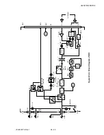
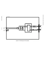
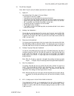
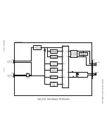
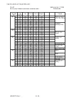
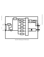
TEL-W2D circuit diagram
TEL-W2D board is for the Germany version only.
1)
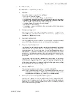
Speech IC
General functions of the speech IC are as follows:
•
Basic speech functions included.
•
Separate receive pre-amplifier with signal output terminal
•
Separate receive power amplifier input terminal, cause it is possible to mixing input.
•
Balanced input for microphone input to provide immunity to common mode noise.
•
MF pre-amplifier input terminal is possible to mixing input.
•
Dial pulse waveform improvement circuit included.
•
Manual pad function included.
•
The transmit, receive, and DTMF amplifiers are provided with AGC in accodance
with the line circuit.
2)
Sending Level Adjustment
The sending level can be adjusted by resistor R55 connected in parallel with the section
in front of the transmitter. Increase the resistor value to lower the sending level, and
decrease the value to raise the level.
3)
Receiving Level Adjustment
The receiving level is determined by the resistor value of R35. Decrease the resistor
value of R35 to lower the receiving level, and increase it to raise the level.
4)
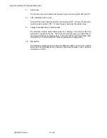
Frequency Response Adjustment
The high range frequency response of the transmitter is determined by the capacitance
of C61. Increase the capacitance of C61 to lower the high range level, and decrease
the capacitance to raise the high range level. The low range frequency response is
determined by the capacitance of C36 and C37. Increase the capacitance of those
capacitors to raise the low range level, and decrease the capacitance to lower the level.
When the capacitance of C36 and C37 are changed, both capacitors should have the
same value.
The high range frequency response of the receiver is determined by the capacitance
of C29. Increase the capacitance of C29 to lower the high range level, and lower the
capacitance to raise the level. The low-range frequency response is determined by the
capacitance of C26. Increase the capacitance to raise the low-range level, and lower
the capacitance to decrease the low-range level.
5)
Side-Tone Adjustment
The side-tone level is determined by the values of R19, R22 and C16.
Note: Changing the side tone level setting affects the sending and receiving levels, the
verification and readjustment of the sending and receiving levels, and the
verification and the readjustment of the side tone level are required.
6)
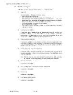
DC V-I (voltage-versus-current) Characteristics Adjustment
The DC V-I characteristics can be changed by mounting or not mounting D10 and D11.
When D10 and D11 are mounted the DC V/I value is raised. When these diodes are
deleted the DC V/I value is lowered. R202 is a 0 W resistor, which is mounted when
D10 and D11 are not being installed.
Содержание OKIFAX 5400
Страница 7: ...40838301TH Rev 1 CHAPTER 1 GENERAL INFORMATION...
Страница 46: ...40838301TH Rev 1 CHAPTER 2 INSTALLATION PROCEDURE...
Страница 130: ...40838301TH Rev 1 CHAPTER 3 BRIEF TECHNICAL DESCRIPTION...
Страница 138: ...40838301TH Rev 1 CHAPTER 4 MECHANICAL DISASSEMBLY AND REASSEMBLY...
Страница 157: ...40838301TH Rev 1 CHAPTER 5 ADJUSTMENTS...
Страница 162: ...40838301TH Rev 1 CHAPTER 6 CLEANING AND MAINTENANCE...
Страница 189: ...40838301TH Rev 1 CHAPTER 7 TROUBLESHOOTING AND REPAIR FOR OKIFAX 5400...
Страница 240: ...40838301TH Rev 1 CHAPTER 8 DIPSWITCHS SETTING TABLES...
Страница 353: ...40838301TH Rev 1 Appendix B Descriptions of Print Operation First Edition August 1999 Oki Data Corporation...
Страница 375: ...40838301TH Rev 1 Appendix C Circuit Diagram and Parts List OK IFAX 5400 First Edition August 1999 Oki Data Corporation...
Страница 380: ...40838301TH Rev 1 D 2 SECTION 1 CABINET ASSEMBLY 5...
Страница 382: ...40838301TH Rev 1 D 4 SECTION 2 CONTROL PANEL ASSEMBLY...
Страница 384: ...40838301TH Rev 1 D 6 SECTION 3 PRINTER ASSEMBLY 51...
Страница 387: ...40838301TH Rev 1 D 9 SECTION 4 BASE ASSEMBLY 30 37 36 39 40 5...
Страница 390: ...40838301TH Rev 1 D 12 SECTION 5 SCAN UNIT...
Страница 392: ...40838301TH Rev 1 D 14 SECTION 6 PAPER GUIDE U ASSEMBLY...
Страница 394: ...40838301TH Rev 1 D 16 SECTION 7 CABLES 10 11 19 12 20 21...
Страница 396: ...40838301TH Rev 1 D 18 SECTION 8 OPTION TELEPHONE US...
Страница 399: ...40838301TH Rev 1 D 21 SECTION 8 OPTION TELEPHONE UK ITA NOR DEN BEL...
Страница 402: ...40838301TH Rev 1 D 24 SECTION 8 OPTION TELEPHONE HOL GER FRA SWITZ AUT INT L...
Страница 405: ...40838301TH Rev 1 Appendix E Board Layout OKIFAX 5400 First Edition August 1999 Oki Data Corporation...
Страница 424: ...40838301TH Rev 1 F 15 5 2 PCB Layout TQSB 2PCB PU FG CONTROLLER MOTOR DRIVER SEN2 MOTOR OSC SEN1...
Страница 425: ...40838301TH Rev 1 F 16 Figure 6 1 6 PARTS LIST SECTION1 CABINET CASSETTE ASSEMBLY F 16 1 4 P 6 5 8 7 3 O 1 2...
Страница 426: ...40838301TH Rev 1 F 17 SECTION2 MECHANICAL ASSEMBLY Figure 6 2 F 16 2 9 A 0 C M L D N E F G H U V T S Q R J I B K A A B B...
Страница 428: ...40838301TH Rev 1 Appendix G RMCS SYSTEM MANUAL For Model 20 First Edition August 1999 Oki Data Corporation...

