CHAPTER 2 CIRCUIT DIAGRAM
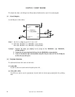
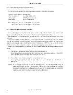
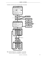
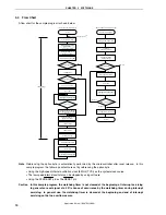
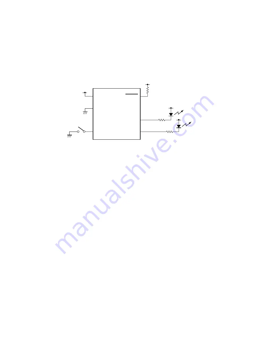
This chapter describes a circuit diagram and the peripheral hardware to be used in this sample program.
2.1 Circuit
Diagram
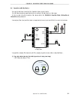
A circuit diagram is shown below.
V
DD
V
DD
Note 1
V
SS
INTP1
Note 2
RESET
P21
P20
V
DD
V
DD
LED2
V
DD
LED1
SW
78K0S/Kx1+
microcontroller
Notes 1.
Use this in a voltage range of 3.0 V
≤
V
DD
≤
5.5 V.
2.
INTP1/P43: 78K0S/KA1+ and 78K0S/KB1+ microcontrollers
INTP1/P32: 78K0S/KY1+ and 78K0S/KU1+ microcontrollers
Cautions 1. Connect the AV
REF
pin directly to V
DD
(only for the 78K0S/KA1+ and 78K0S/KB1+
microcontrollers).
2. Connect the AV
SS
pin directly to GND (only for the 78K0S/KB1+ microcontroller).
3. Leave all unused pins open (unconnected), except for the pins shown in the circuit diagram
and the AV
REF
and AV
SS
pins.
2.2 Peripheral
Hardware
The peripheral hardware to be used is shown below.
(1) Switch (SW)
A switch is used as an input to control the lighting of an LED.
(2) LEDs (LED1, LED2)
The LEDs are used as outputs corresponding to switch inputs and reset signals generated by the watchdog
timer.
Application Note U18847EJ1V0AN
6

