


3- 36
MC68306 USER'S MANUAL
MOTOROLA
ADDR
UDS/LDS
R/W
AS
CLOCK
DTACK
6
S0
S1
S2
S3
S4
S5
S6
S7
S0
18
DATA
23
53
47
9
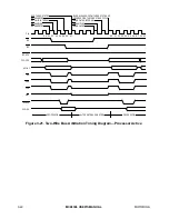
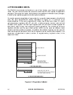
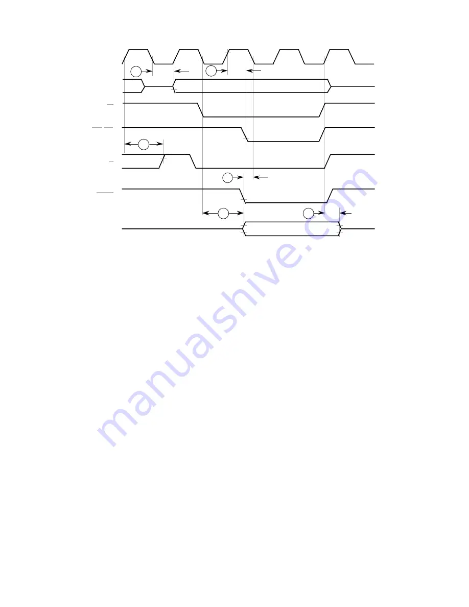
Figure 3-33. Synchronous Write Cycle
A key consideration when designing in a synchronous environment is the timing for the
assertion of
DTACK
and
BERR
by an external device. To properly use external inputs, the
processor must synchronize these signals to the internal clock. The processor must
sample the external signal, which has no defined phase relationship to the CPU clock,
which may be changing at sampling time, and must determine whether to consider the
signal high or low during the succeeding clock period. Successful synchronization requires
that the internal machine receives a valid logic level, whether the input is high, low, or in
transition.
Parameter #47 of AC Electrical Specifications—Read and Write Cycles is the
asynchronous input setup time. Signals that meet parameter #47 are guaranteed to be
recognized at the next falling edge of the system clock. However, signals that do not meet
parameter #47 are not guaranteed to be recognized. In addition, if
DTACK
is recognized
on a falling edge, valid data is latched into the processor (during a read cycle) on the next
falling edge, provided the data meets the setup time required (parameter #27). When
parameter #27 has been met, parameter #31 may be ignored. If
DTACK
is asserted with
the required setup time before the falling edge of S4, no wait states are incurred, and the
bus cycle runs at its maximum speed of four clock periods.