


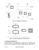


8- 8
MC68306 USER'S MANUAL
MOTOROLA
8
15
13
9
14
12
17
18
47
28
25
26
48
47
30
47
32
56
47
32
S0
S1
S2
S3
S4
S5
S6
CLKOUT
FC2–FC0
A23–A1
AS
LDS / UDS
R/W
DTACK
DATA OUT
BERR / BR
(NOTE 3)
HALT / RESET
47
ASYNCHRONOUS
INPUTS
(NOTE 1)
S7
23
7
11
9
53
55
21
22
20
11A
2. Because of loading variations, R/W may be valid after AS even though both are initiated by the rising edge
of S2 (specification #20A).
14A
20A
UW, LW
NOTES:
1. Setup time (#47) for asynchronous inputs (
HALT, RESET, BR, BGACK, DTACK, BERR,
IRQx
)
guarantees
their recognition at the next falling edge of the clock.
3. BR need fall at this time only to ensure being recognized at the end of the bus cycle.
(NOTE 2)
(NOTE 2)
15A
9A
12A
6
Figure 8-4. Write Cycle Timing Diagram