


MOTOROLA
MC68306 USER'S MANUAL
3- 25
(
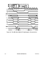
BERR
alone). As long as
BERR
remains asserted, the data bus is in the high-impedance
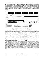
state. Figure 3-24 shows the timing for the normal bus error.
S0
S2
S4
S6
CLK
FC2–FC0
A31–A1
w
w
w
w
S8
AS
LDS/UDS
R/W
DTACK
D15–D0
BERR
HALT
INITIATE
BUS ERROR
DETECTION
INITIATE BUS
ERROR STACKING
RESPONSE
FAILURE
READ
Figure 3-24. Bus Error Timing Diagram
After the aborted bus cycle is terminated and
BERR
is negated, the processor enters
exception processing for the bus error exception. During the exception processing
sequence, the following information is placed on the supervisor stack:
1. Status register
2. Program counter (two words, which may be up to five words past the instruction
being executed)
3. Error information
The first two items are identical to the information stacked by any other exception. The
EC000 core stacks bus error information to help determine and to correct the error.
After the processor has placed the required information on the stack, the bus error
exception vector is read from vector table entry 2 (offset $08) and placed in the program
counter. The processor resumes execution at the address in the vector, which is the first
instruction in the bus error handler routine.
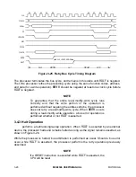
3.4.2 Retrying the Bus Cycle
The assertion of the bus error signal during a bus cycle in which
HALT
is also asserted by
an external device initiates a retry operation. Figure 3-25 is a timing diagram of the retry
operation.