


8- 6
MC68306 USER'S MANUAL
MOTOROLA
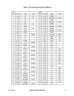
8.7 AC ELECTRICAL SPECIFICATIONS—READ AND WRITE
CYCLES
(Continued)
16.67 MHz
Num
Characteristic
Min
Max
Unit
20A
6
AS
Asserted to R/
W
Low (Write)
—
10
ns
21
2
Address Valid to R/
W
Low (Write)
0
—
ns
21A
2
FC Valid to R/
W
Low (Write)
30
—
ns
22
2
R/
W
Low to
LDS, UDS
Asserted (Write)
30
—
ns
23
CLKOUT Low to Data-Out Valid (Write)
—
30
ns
25
2
AS, LDS, UDS
Negated to Data-Out Invalid (Write)
15
—
ns
26
2
Data-Out Valid to
LDS, UDS
Asserted (Write)
15
—
ns
27
5
Data-In Valid to CLKOUT Low (Setup Time on Read)
5
—
ns
28
2
AS, LDS, UDS
Negated to
DTACK
Negated (Asynchronous
Hold)
0
110
ns
29
AS, LDS, UDS
Negated to Data-In Invalid (Hold Time on Read)
0
—
ns
29A
AS, LDS, UDS
Negated to Data-In High Impedance
—
90
ns
30
AS, LDS, UDS
Negated to
BERR
Negated
0
—
ns
312,5
DTACK
Asserted to Data-In Valid (Setup Time)
—
50
ns
32
HALT
and
RESET
Input Transition Time
—
150
ns
475
Asynchronous Input Setup Time
5
—
ns
483
BERR
Asserted to
DTACK
Asserted
10
—
ns
53
Data-Out Hold from CLKOUT High
0
—
ns
55
R/
W
Asserted to Data Bus Impedance Change
0
—
ns
564
HALT/RESET
Pulse Width
10
—
Clks
NOTES:
1.
For a loading capacitance of less than or equal to 50 pF, subtract 5 ns from the value given in the
maximum columns.
2.
Actual value depends on clock period.
3.
If #47 is satisfied for both
DTACK
and
BERR
, #48 may be ignored. In the absence of
DTACK, BERR
is an asynchronous input using the asynchronous input setup time (#47).
4. For power-up, the MC68306 must be held in the reset state for 100 ms to allow stabilization of on-chip
circuitry. After the system is powered up, #56 refers to the minimum pulse width required to reset the
controller.
5.
If the asynchronous input setup time (#47) requirement is satisfied for
DTACK
, the
DTACK
asserted to data
setup time (#31) requirement can be ignored. The data must only satisfy the data-in to clock low setup time
(#27) for the following clock cycle.
6.
When
AS
and R/
W
are equally loaded (
±
20%), subtract 5 ns from the values given in these columns.
7.
The processor will negate
BG a
nd begin driving the bus again if external arbitration logic negates
BR
before
asserting
BGACK.
8.
The minimum value must be met to guarantee proper operation. If the maximum value is exceeded,
BG
may be
reasserted.
9.
AS
is always asserted, regardless of whether it is mapped to internal or external resources. If the designer
wishes to decode more chip selects than are provided, use one of CS0–7 as the enable for the external decode.