


3- 28
MC68306 USER'S MANUAL
MOTOROLA
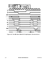
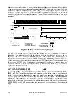
After the processor is reset, it reads the reset vector table entry (address $00000) and
loads the contents into the supervisor stack pointer (SSP). Next, the processor loads the
contents of address $00004 (vector table entry 1) into the program counter. Then the
processor initializes the interrupt level in the status register to a value of seven. No other
register is affected by the reset sequence. Figure 3-27 shows the timing of the reset
operation.
T 4 CLOCKS
2
3
4
5
6
NOTES:
1. Internal start-up time
2. SSP high read in here
3. SSP low read in here
4. PC High read in here
5. PC Low read in here
6. First instruction fetched here
Bus State Unknown:
All Control Signals Inactive.
Data Bus in Read Mode:
CLK
+ 5 VOLTS
VCC
RESET
HALT
BUS CYCLES
<
T 100 MILLISECONDS
≥
1
Figure 3-27. Reset Operation Timing Diagram
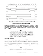
The active-low
RESET
signal is asserted by the EC000 core when a RESET instruction is
executed. This signal should reset all external devices (the EC000 core itself is not
affected). The processor drives
RESET
for 124 clock periods. The
RESET
signal is
asserted by an external source to reset the EC000 core.
RESET
by itself will reset the
EC000 core unless the processor is executing a RESET instruction. To guarantee a reset
of the core,
RESET
must be asserted for at least 132 clocks (i.e., longer than the
maximum duration of the RESET instruction), or
RESET
and
HALT
must be asserted
together for at least 10 clocks.
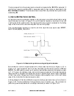
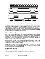
3.6 THE RELATIONSHIP OF
DTACK
,
BERR
, AND
HALT
To properly control termination of a bus cycle for a retry or a bus error condition,
DTACK
,
BERR
, and
HALT
should be asserted and negated on the rising edge of the processor
clock. This relationship assures that when two signals are asserted simultaneously, the
required setup time (specification #47, AC Electrical Specifications
Ñ
Read and Write
Cycles) for both of them is met during the same bus state. External circuitry should be
designed to incorporate this precaution. A related specification, #48, can be ignored when
DTACK
,
BERR
, and
HALT
are asserted and negated on the rising edge of the processor
clock.