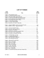
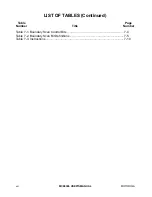


2- 8
MC68306 USER'S MANUAL
MOTOROLA
additional information about the interaction between
HALT
and
RESET
, refer to 3.5 Reset
Operation and for more information on
HALT
and
BERR
, refer to 3.4 Bus Error and Halt
Operation.
Processor assertion of
HALT
indicates a double bus fault condition. This condition is
unrecoverable; the MC68306 must be externally reset to resume operation.
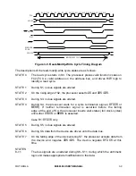
2.1.12 Read/Write (R/
W
)
This three-state, bi-directional signal defines the data bus transfer as a read or write cycle.
The R/
W
signal relates to the data strobe signals described in the following paragraphs.
2.1.13 Upper And Lower Data Strobes (
UDS
,
LDS
)
These three-state, bi-directional signals and R/
W
control the flow of data on the data bus.
Table 2-9 lists the combinations of these signals, the corresponding data on the bus, and
the
OE, LW,
and
UW
signals. When the R/
W
line is high, the processor reads from the
data bus. When the R/
W
line is low, the processor drives the data bus. When another bus
master controls the bus, the
UDS, LDS,
and R/
W
pins become inputs and the
OE, LW,
and
UW
signals are still decoded as shown in Table 2-9.
Table 2-9. Data Strobe Control of Data Bus
UDS
LDS
R/
W
D8–D15
D0–D7
OE
UW
LW
High
High
—
No Valid Data
No Valid Data
High
High
High
Low
Low
High
Valid Data Bits
15–8
Valid Data Bits
7–0
Low
High
High
High
Low
High
No Valid Data
Valid Data Bits
7–0
Low
High
High
Low
High
High
Valid Data Bits
15–8
No Valid Data
Low
High
High
Low
Low
Low
Valid Data Bits
15–8
Valid Data Bits
7–0
High
Low
Low
High
Low
Low
Valid Data Bits
7–0*
Valid Data Bits
7–0
High
High
Low
Low
High
Low
Valid Data Bits
15–8
Valid Data Bits
15–8*
High
Low
High
*These conditions are a result of current implementation and may not appear
on future devices.
2.1.14 Upper-Byte Write (
UW
)
This signal is a combination of R/
W
low and
UDS
low for writing the upper-byte of a 16-bit
port. This signal simplifies memory system design by explicitly signalling that data is valid
on the upper portion of the data bus on a write operation.
UW
is also decoded for external
bus masters.