LTC3882-1
43
Rev A
APPLICATIONS INFORMATION
The minimum saturation current rating should be chosen
to allow margin due to manufacturing and temperature
variation in the sense resistor or inductor DCR. A reason-
able I
SAT
value would be 2.2 • I
OUT
.
The programmed current limit IOUT_OC_FAULT_LIMIT
must be low enough to ensure that the inductor never
saturates and high enough to allow increased current
during transient conditions with margin for DCR variation.
For example, if
I
SAT
= 2.2 • I
OUT
, and
I
MAX
= 1.6 • I
OUT
a reasonable output current limit would be
IOUT_OC_FAULT_LIMIT = 1.8 • I
OUT
Once the value of L is known, the type of inductor must be
selected. High efficiency converters generally cannot afford
the core losses found in low cost powdered iron cores,
forcing the use of more expensive ferrite or molypermalloy
cores. Also, core losses decrease as inductance increases.
Unfortunately, increased inductance requires more turns
of wire, larger inductance and larger copper losses.
Ferrite designs have very low core loss and are preferred at
high switching frequencies. However, these core materials
exhibit hard saturation, causing an abrupt reduction in the
inductance when the peak current capability is exceeded.
Do not allow the core to saturate!
Power MOSFET Selection
The LTC3882-1 requires at least two external N-channel
power MOSFETs per channel, one for the top (main) switch
and one or more for the bottom (synchronous) switch. The
number, type and on-resistance of the MOSFETs selected
should take into account the voltage step-down ratio and
the FET circuit position (main or synchronous switch).
A much smaller and lower input capacitance MOSFET
should be used for the top MOSFET in applications that
have an output voltage that is less than one-third of the
input voltage. At operating frequencies above 300kHz
and where V
IN
>> V
OUT
, the top MOSFET on-resistance
is normally less important for overall efficiency than its
input capacitance. MOSFET manufacturers have designed
special purpose devices that provide reasonably low on-
resistance with significantly reduced input capacitance
for the main switch application in switching regulators.
Selection criteria for the power MOSFETs include on-
resistance, gate charge, Miller capacitance, breakdown
voltage and maximum output current.
For maximum efficiency, R
DS(ON)
and Q
G
should be mini-
mized. Low R
DS(ON)
minimizes conduction losses and low
Q
G
minimizes switching and transition losses. MOSFET
gate charge can be taken from the typical gate charge
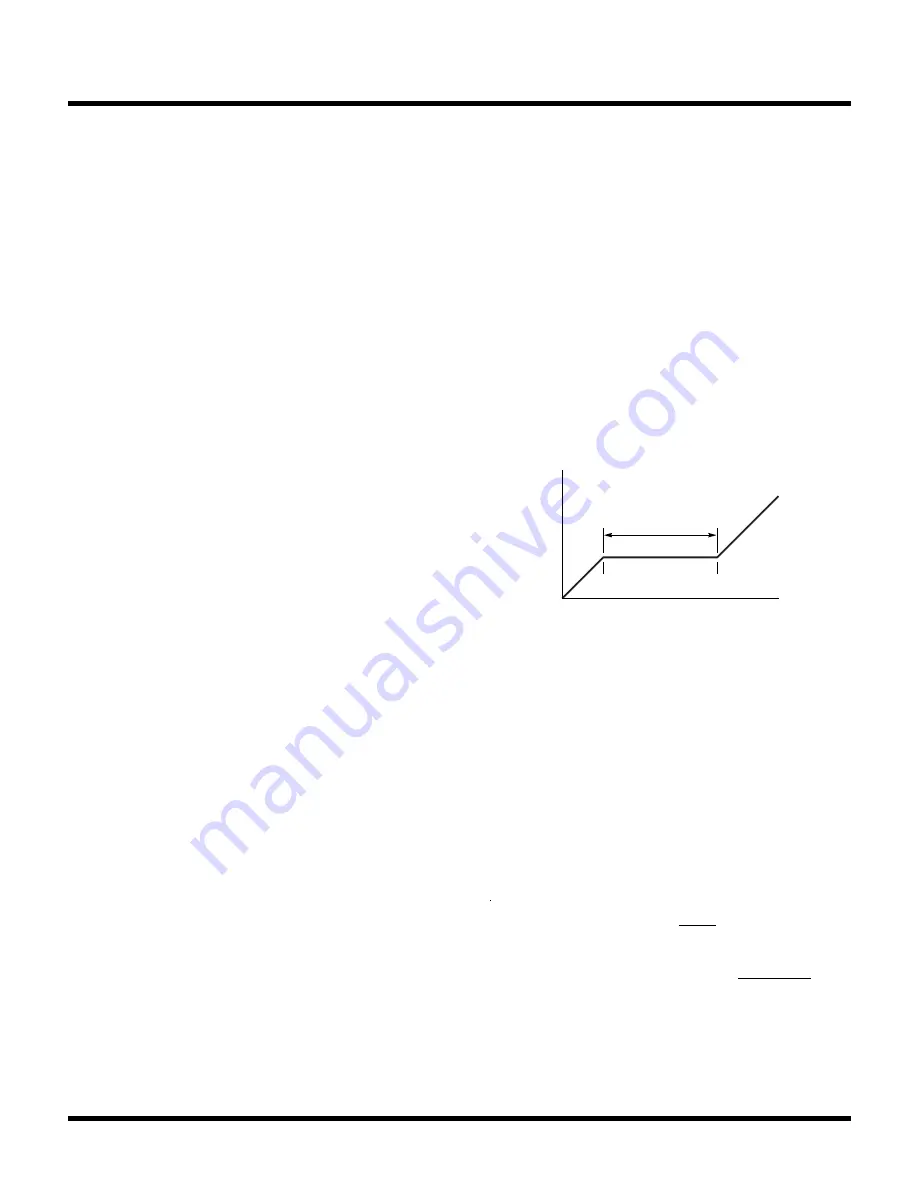
curve included on most data sheets (Figure 21).
Figure 21. Typical MOSFET Gate Charge Curve
C
MILLER
is the most important selection criteria for deter-
mining the transition loss term in the top MOSFET but is
not directly specified on MOSFET data sheets. C
MILLER
is
equal to the increase in gate charge along the horizontal
axis of Figure 21 while the curve is approximately flat,
divided by the specified change in V
DS
. This result is
then multiplied by the ratio of the actual application V
DS
to the V
DS
specified on the gate charge curve. When the
controller is operating in continuous mode the duty cycles
for the top and bottom MOSFETs are given by:
Main Switch Duty Cycle
=
V
OUT
V
IN
Synchronous Switch Duty Cycle
=
V
IN
– V
OUT
V
IN
38821 F21
MILLER EFFECT
Q
IN
C
MILLER = (
Q
B –
Q
A)/
V
DS
V
GS
Q
A
Q
B


