214
Intel
®
855GME Chipset and Intel
®
6300ESB ICH Embedded Platform Design Guide
Intel
®
6300ESB Design Guidelines
When crossing a plane split is completely unavoidable, proper placement of stitching caps may
minimize the adverse effects on EMI and signal quality performance caused by crossing the split.
Stitching capacitors are small-valued capacitors (1 µF or lower in value) that bridge voltage plane
splits close to where High-speed signals or clocks cross the plane split. The capacitor ends should
tie to each plane separated by the split. They are also used to bridge, or bypass, power and ground
planes close to where a high-speed signal changes layers. As an example of bridging plane splits, a
plane split that separates V
CC
5 and V
CC
3.3 planes should have a stitching cap placed near any
high-speed signal crossing. One side of the cap should tie to V
CC
5 and the other side should tie to
V
CC
3.3. Stitching caps provide a high frequency current return path across plane splits. They
minimize the impedance discontinuity and current loop area that crossing a plane split creates.
9.6.2.2
GND Plane Splits, Voids, and Cut-Outs (Anti-Etch)
Avoid anti-etch on the GND plane.
9.6.3
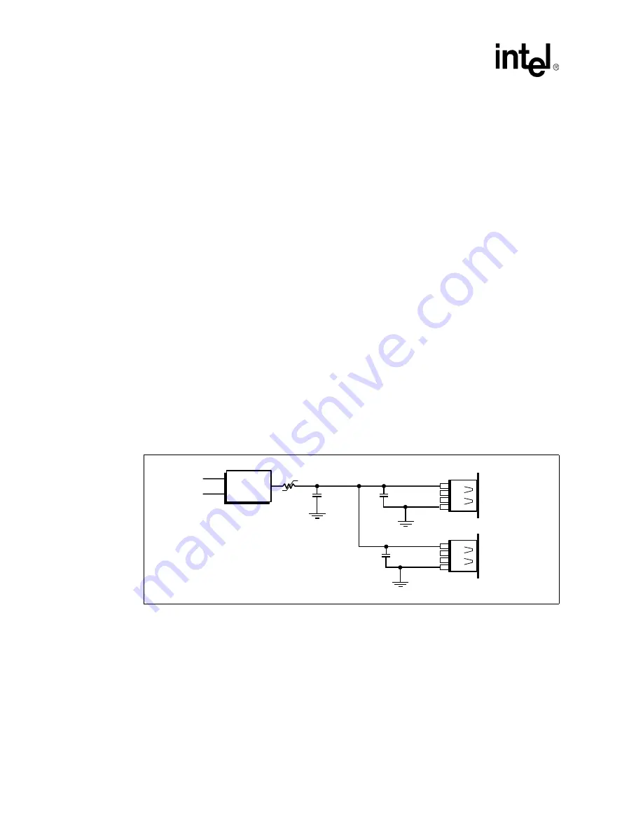
USB Power Line Layout Topology
The following is a suggested topology for power distribution of V
BUS
to USB ports. Circuits of this
type provide two types of protection during dynamic attach and detach situations on the bus: inrush
current limiting (droop) and dynamic detach fly back protection. These two different situations
require both bulk capacitance (droop) and filtering capacitance (for dynamic detach fly back
voltage filtering). It is important to minimize the inductance and resistance between the coupling
capacitors and the USB ports. That is, capacitors should be placed as close as possible to the port
and the power-carrying traces should be as wide as possible, preferably, a plane. Make the
power-carrying traces wide enough that the system fuse will blow on an over current event. When
the system fuse is rated at 1 amps, the power-carrying traces should be wide enough to carry at
least 1.5 amps.
9.6.4
EMI Considerations
The following guidelines apply to the selection and placement of common mode chokes and ESD
protection devices.
Figure 110.
Good Downstream Power Connection
B1162-01
5 V
Switch
5 V
5 V Sus
Thermister
220µF
470pF
Port 1
V
CC
GND
1
4
470pF
Port 2
V
CC
GND
1
4
Содержание 6300ESB ICH
Страница 24: ...24 Intel 855GME Chipset and Intel 6300ESB ICH Embedded Platform Design Guide Introduction...
Страница 36: ...36 Intel 855GME Chipset and Intel 6300ESB ICH Embedded Platform Design Guide General Design Considerations...
Страница 102: ...102 Intel 855GME Chipset and Intel 6300ESB ICH Embedded Platform Design Guide...
Страница 122: ...122 Intel 855GME Chipset and Intel 6300ESB ICH Embedded Platform Design Guide...
Страница 152: ...152 Intel 855GME Chipset and Intel 6300ESB ICH Embedded Platform Design Guide System Memory Design Guidelines DDR SDRAM...
Страница 172: ...172 Intel 855GME Chipset and Intel 6300ESB ICH Embedded Platform Design Guide Integrated Graphics Display Port...
Страница 190: ...190 Intel 855GME Chipset and Intel 6300ESB ICH Embedded Platform Design Guide Hub Interface...
Страница 246: ...246 Intel 855GME Chipset and Intel 6300ESB ICH Embedded Platform Design Guide Intel 6300ESB Design Guidelines...
Страница 264: ...264 Intel 855GME Chipset and Intel 6300ESB ICH Embedded Platform Design Guide Platform Clock Routing Guidelines...
Страница 298: ...298 Intel 855GME Chipset and Intel 6300ESB ICH Embedded Platform Design Guide Schematic Checklist Summary...
Страница 318: ...318 Intel 855GME Chipset and Intel 6300ESB ICH Embedded Platform Design Guide Layout Checklist...


