Rev. 1.10
108
November 04, 2019
Rev. 1.10
109
November 04, 2019
HT45F5Q-3
Battery Charger Flash MCU
HT45F5Q-3
Battery Charger Flash MCU
I
2
C Interface Operation
The I
2
C serial interface is a two line interface, a serial data line, SDA, and serial clock line, SCL. As
many devices may be connected together on the same bus, their outputs are both open drain types.
For this reason it is necessary that external pull-high resistors are connected to these outputs. Note
that no chip select line exists, as each device on the I
2
C bus is identified by a unique address which
will be transmitted and received on the I
2
C bus.
When two devices communicate with each other on the bidirectional I
2
C bus, one is known as the
master device and one as the slave device. Both master and slave can transmit and receive data,
however, it is the master device that has overall control of the bus. For the device, which only
operates in slave mode, there are two methods of transferring data on the I
2
C bus, the slave transmit
mode and the slave receive mode. The pull-high control function pin-shared with SCL/SDA pin is
still applicable even if I
2
C device is activated and the related internal pull-high register could be
controlled by its corresponding pull-high control register.
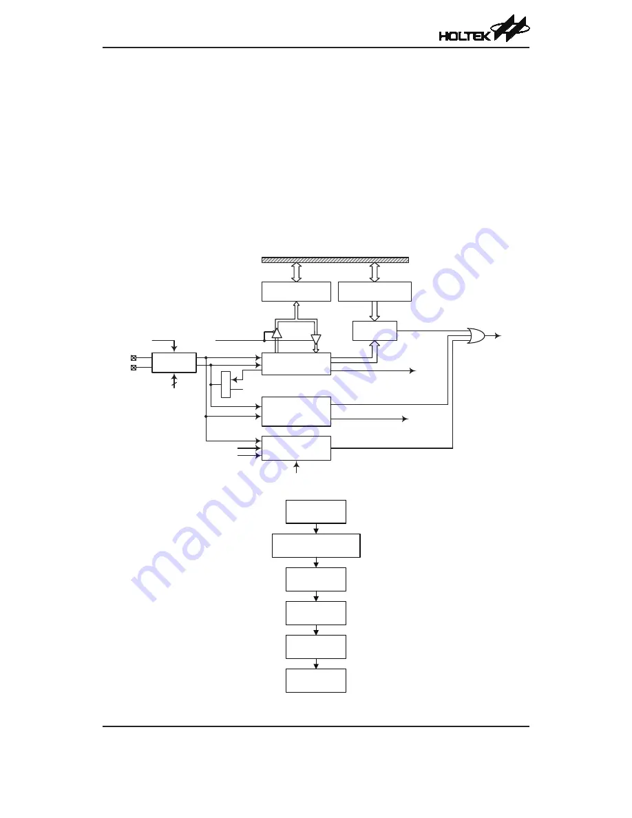
Shift Register
Transmit/
Receive
Control Unit
f
SYS
f
SUB
Data Bus
I
2
C Address Register
(SIMA)
I
2
C Data Register
(SIMD)
Address
Comparator
Read/Write Slave
SRW
Detect Start or Stop
HBB
Time-out
Control
SIMTOF
Address Match
–
HAAS
USIM
Interrupt
Debounce
Circuitry
SCL Pin
M
U
X
TXAK
Data out MSB
SIMTOEN
Address Match
SIMDEB[1:0]
SDA Pin
Data in MSB
Direction Control
HTX
8-bit Data Transfer Complete
–
HCF
I
2
C Block Diagram
START signal
from Master
Send slave address
and R/W bit from Master
Acknowledge
from slave
Send data byte
from Master
Acknowledge
from slave
STOP signal
from Master


