28
FinePix S602 ZOOM SERVICE MANUAL
3. Schematic
3-3.Functions of Primary Blocks
3-3-1.Technical Outline
Use of
[the 3rd Generation Super CCD Honeycomb]
has improved still photography performance. The 3,100,000
effective pixels, and [the Honeycomb Signal Processing System], allows recording and reproduction of high-quality
images of up to 2832 x 2128 (6,030,000) pixels. These features permit
[Candle Shots]
at ISO1600/800 in the 1Mega
mode, a capability facilitated by the use of the unique honeycomb picture element which receives light over a wide
area, technical developments in
pixel summing signal processing*1
, and noise reduction technology.
Movie photography performance is improved.
Horizontal/vertical pixel mixing*2
inside the CCD using a new data
transfer system is the first to provide 30 frames per second in VGA format at greater than 3 megapixels.
[High-speed Twin AF]
uses both an external AF sensor (passive phase difference) and the CCD AF for higher-speed
autofocus.
The
[Super Macro]
feature allows photography of a subject at distances down to one centimeter.
The
[Double Slot]
feature provides for both smart media and microdrives, allowing both recording of the large
volumes of image data in the high image quality mode, and long movies.
*1
: Image data obtained with honeycomb signal processing from twice the number of effective pixels. Shrinks four
pixels into one. This processing increases the signal level (sensitivity) by a factor of four, and the S/N ratio (signal-to-
noise ratio) by a factor of two, to permit photography at ISO1600.
*2
: Mixes two pixels on the vertical axis, and two pixels on the horizontal axis, of the CCD.
This processing increases the signal level by a factor of four, and the S/N ratio by a factor of two, to provide high
sensitivity and high quality images, while at the same time allowing data to be read at high-speed (30 frames per
second in VGA format).
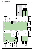
3-3-2.CAM Board Block Functions
Photography Circuit Functions (CAM BLOCK)
The analog video signal output from the newly developed CCD (1/1.7”, 3,100,000 effective pixels, square pixel
honeycomb array, primary color CCD) is processed (pseudo-color compensation, adaptive interpolation, amplifica-
tion, and signal mixing) in
SCS3A_IC (IC102:CSP_IC)
, and subsequently converted to a 12-bit digital signal. The
digital signal is then sent to the single chip image signal processing LSI :
UCS1_IC (IC210 : CSP_IC*)
.
* CSP_IC
=
C
hip
S
ize
P
ackege
IC
3-3-3.MAIN Board Block Functions
Image Signal Processing Functions (PROCESS BLOCK)
Data input from CCD
* The 12-bit digital image data (1H equivalent) output from the CAM BLOCK is sent to
UCS1_IC
, buffered in the IBUF,
and converted to 32-bit (16-bit x 2) data. The 32-bit image data is then sent from the [I/O Buffer] in
UCS1_IC
and
stored in the
SDRAM_IC (IC211, IC218, IC219 : 40 Mbyte
). A single frame (2832 pixels x 2128 lines) of image data is
temporarily stored in the
SDRAM_IC
.
* At the same time, AE multiplies the 12-bit image data input from the
UCS1_IC
in [AUTO], and sends the data required
for AE/AWB/AF to the
SDRAM_IC
. To provide the appropriate data for AE/AWB/AF, this data is then sent from the
SDRAM_IC
in serial format to the
SCS3A_IC
via the
UCS1_IC
.
Recording in the SSFDC
The image data stored in the
SDRAM_IC
is converted from 32-bit to 12-bit data one line at a time in the [IBUF] in the
UCS1_IC
, and sent to [YC PRO]. The image data is then converted to 8-bit Y and C signals in [YC PRO], and then sent
again to [IBUF]. The 8-bit Y and C signals are then converted to 8-bit Y, Y, Cb, and Cr signals and sent to the
SDRAM_IC
.
The image data stored in the
SDRAM_IC
is compressed with [JPEG] in the
UCS1_IC
and again stored in the
SDRAM_IC
. The image data following compression is recorded sequentially in the SSFDC via [MEDIA] in the
UCS1_IC
.
Image Replay from the SSFDC
The compressed image data from the SSFDC is sent to
UCS1_IC
, and stored in the
SDRAM_IC
via [MEDIA]. The
compressed image data stored in the
SDRAM_IC
is expanded with JPEG and stored again in the
SDRAM_IC
. The
expanded image data is sent to [YC PRO] via [IBUF]. Gain control for the luminance and color difference signals, and
aperture processing, are performed in [YC PRO] and the image data then sent again to the
SDRAM_IC
. The image
data is then displayed via [ENCD] and [D/A].
Movie Mode
The 12 bit digital image data output from the (CAM BLOCK) is converted to 8-bit Y and C signals in the
USC1_IC
[YC
PRO], and sent to the
SDRAM_IC
. The image data stored in the
SDRAM_IC
is compressed with [JPEG] in the
UCS1_IC
and again stored in the
SDRAM_IC
. The image data following compression is recorded sequentially in the
SSFDC via [MEDIA] in the
UCS1_IC
.
The photography adjustment data is stored in the
FLASH_ROM (IC216)
. The
FLASH_ROM
also incorporates firmware.
LCD Control Functions (LCD CONTROL BLOCK)
The R, G, and B signals processed in the image signal processing
UCS1_IC
are output to the LCD panel via [LCD CONT].
A low-temperature polysilicon TFT color LCD monitor (1.8, 110,000 pixels) is used.
EVF Control Functions (EVF CONTROL BLOCK)
The R, G, and B signals processed in the image signal processing
UCS1_IC
are output to the EVF panel via [EVF CONT].
A high-temperature polysilicon TFT color monitor (0.44, 180,000 pixels) is used in the viewfinder.
3-3-4.DCTS Board Block Functions
Power Supply Functions
The power supply circuit on the DCST board generates the
-8V/16V
(CCD),
1.5V
(UCS1_IC),
3.3V
(SCS3A_IC/UCS1_IC/SDRAM/SDRAM/ROM/LED/KEY),
MOT_5.0V
(lens/flash),
D_5V
(AUD01),
LCD_13V
(LCD/EVF
backlight),
D_3.3V
(LCD circuit), and
AD_3.3V
(video circuit) voltages.

