


M
ODEL
SDP100 V
ERSION
V_1.00
P
REPARED BY
H/W
D
ATE
25/05/2007
S
UBJECT
T
ECHNICAL
M
ANUAL
P
AGE
68/70
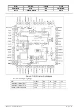
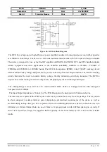
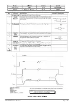
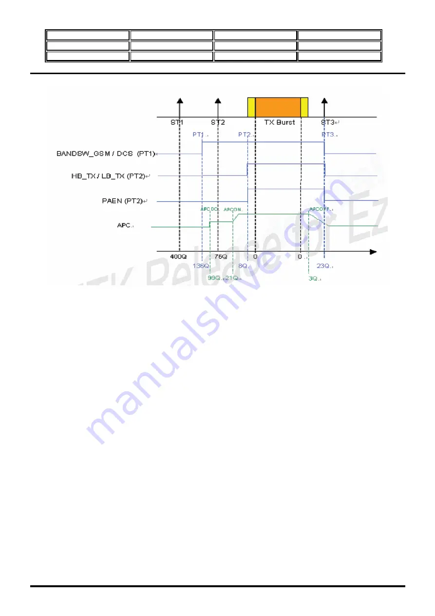
The Next Picture is for RF TX Timing of BSI and BPI.
< Single Slot TX Event with Timing Requirement>
<BSI Interface>
In order to simply the serial control mechanism, and achieve best usage of BSI resources. Each burst transmitted,
There are three generic timing defined (ST1/ST2/ST3) to send 3-wire control commands to transceiver. Usually
1’st BSI event(ST1) is used to warm up the synthesizer and set its N-counter to lock the operational frequency. The
2’nd BSI(ST2) is used to set the transmitted mode and indicate the operational band. The 3’rd BSI(ST3)is used to
command transceiver entering idle mode. All bands(GSM/DCS/PCS) share the same timing.
<BPI interface>
In order to simply the parallel control mechanism, and achieve best usage of BPI resources. Each burst transmitted,
there are also three generic timing defined(PT1/PT2/PT3) to send HW control Signals to RF module. In other
words, there are only three timing events to trigger HW control signals changing their states. Usually 1’st BPI
event(PT1) is used to select suitable band for TXVCO. The 2’nd BPI(PT2) is used to turn on PA and control
antenna switch depends on its band. The 3’rd BSI(ST3) is used to force RF module to terminate transmission and
enter idle mode. All bands share the same timing but could has different HW control signals.
SDP100
T
ECHNICAL
M
ANUAL
Page 3.68