


M
ODEL
SDP100 V
ERSION
V_1.00
P
REPARED BY
H/W
D
ATE
25/05/2007
S
UBJECT
T
ECHNICAL
M
ANUAL
P
AGE
47/70
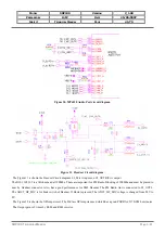
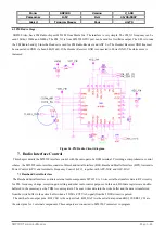
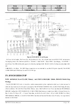
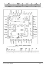
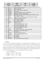
Figure 37. The AFC and VCTCXO Circiut diagram
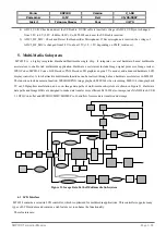
8.
Clocks and Reset
Clocks
There are two major time bases in the MT6228. For the faster one is the 13MHz clock origination from an off-chip
temperature-compensated voltage controlled oscillator that can be 26MHz. This signal is the input from the SYSCLK pad then
is converted to the square-wave signal. The other time base is the 32.768KHz clock generated by an on-chip oscillator
connected to an external crystal.
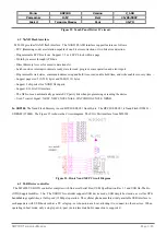
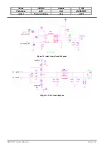
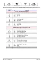
- 32.768Khz Time Base
The 32.768Khz clock is always running. It’s mainly used as the time base of the Real Time Clock(RTC) module,
which maintains time and date with counters. In low power mode, the 13Mhz time base is turned off, so the
32.768Khz clock shall be employed to update the critical TDMA timer and Watchdog timer. This Time base is also
used to clock the keypad Scanner logic. The C101,C102 must be tuned with Oscillator.
- 13Mhz Time Base
Two 1/2-dividers, one for MCU Clock and the other for DSP Clock, exist to allow usage of either 26 or 13Mhz
TXVCXO as clock input. There phase-locked loops(MPLL, DPLL and UPLL) are used to generate three primary
clocks.
MPLL : Provides the MCU System Clock.
DPLL : Provides the DSP System Clock. DPLL can be programmed to provide 1x to 6x
output of the 13Mhz reference.
UPLL : Provides the USB System Clock.
Reset Generation Unit
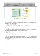
Figure 38 shows reset scheme used in MT6228. There are three kinds of resets in the MT6228, i.e., hardware reset, watchdog
reset, and software resets.
SDP100
T
ECHNICAL
M
ANUAL
Page 3.47