


M
ODEL
SDP100 V
ERSION
V_1.00
P
REPARED BY
H/W
D
ATE
25/05/2007
S
UBJECT
T
ECHNICAL
M
ANUAL
P
AGE
54/70
SDP100
T
ECHNICAL
M
ANUAL
Page 3.54
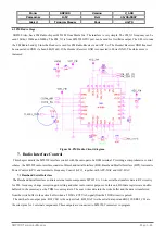
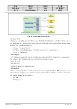
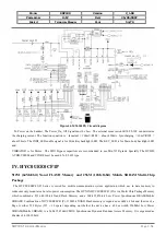
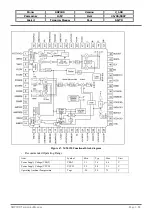
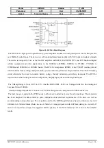
Figure 44. MT6305BN Circuit diagram
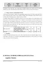
To Power on the handset, The Power_On_Off Signal must be Low. The external sense resistor R302 0.39F can determine
the charging current. The function equation is : Iconstant = 160mV/R302 = about 450mA. Ipre-charging = 10mV/R302 =
about 24mA. The INDI_LED enable signal is for Slide Key backlight LED, The KEY_LED is for Main body backlight LED
and
VIBRATOR is for Motor. The LDO Bypass capacitors are recommended to use Min X5R grade. Specially The DVDD,
AVDD,VMEM and VCORE must be used 4.7uF, 2012 type.
IV. HYC0UEE0CF1P
512M (64Mx8bit) Nand FLASH Memory and 256M (16Mx16bit) Mobile SDRAM Multi-Chip
Package
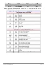
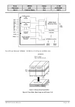
The HYC0UEE0CF1(P) Series is suited for mobile communication system application which use in data memory to
reducenot only mount area but also power consumption. The HYNIX HYC0UEE0CF1(P) is is a Multi Chip Package Memory
which combined a 553,648,128-bit Nand Flash Memory and a 268,435,456-bit Low Power Synchronous DRAM(Mobile
SDRAM). Combination of HYC0UEE0CF1(P), 512Mbit NAND Flash memory is organized as 64M x8 bits and the size of a
Page is either 528 Bytes (512 + 16 spare) depending on whether the device has a x8 bus width. 256Mbit Low Power
SDRAM(Mobile SDRAM) is a 268,435,456bit CMOS Synchronous Dynamic Random Access Memory. It is organized as
4banks of 4,194,304x16.