


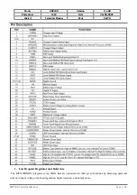


M
ODEL
SDP100 V
ERSION
V_1.00
P
REPARED BY
H/W
D
ATE
25/05/2007
S
UBJECT
T
ECHNICAL
M
ANUAL
P
AGE
37/70
SDP100
T
ECHNICAL
M
ANUAL
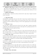
Page 3.37
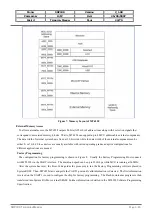
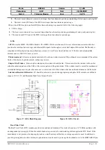
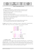
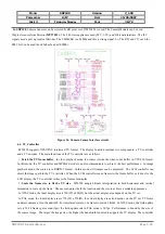
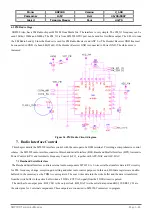
Figure 25. Card Detection.
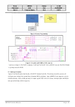
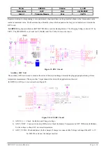
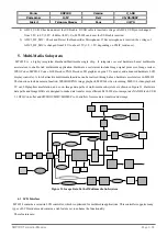
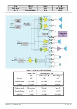
6.5
Camera Interface
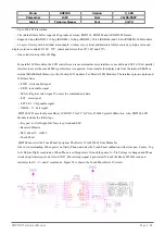
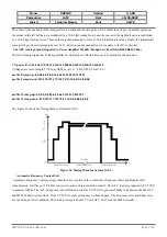
MT6228 incorporates a feature rich image signal processor to connect with a variety of image sensor components. This
processor(ISP) consists of timing generated unit (TG) and lens/sensor compensation unit and image process unit. Timing
generated unit (TG) cooperates with master type image sensor only. That means sensor should send vertical and
horizontal signals to TG. TG offers sensor required data clock and receive sensor Bayer pattern raw data by internal auto
synchronization or external pixel clock synchronization. The main purpose of TG is to create data clock for master type
image sensor and accept vertical/horizontal synchronization signal and sensor data, and then generate grabbed area of raw
data or YUV422/RGB565 data to the lens/sensor compensation unit. Lens/sensor compensation unit generates
compensated raw data to the colour process unit in Bayer raw data input mode. In YUV422/RGB565 input mode, this
stage is bypassed. Image process unit accepts Bayer pattern raw data or YUV422/RGB565 data that is generated by
lens/sensor compensation unit. The output of ISP is YCbCr 888 data format which can be easily encoded by the compress
engine (JPEG encoder and MPEG4 encoder). It can be the basic data domain of other data format translation such as
R/G/B domain. The ISP is pipelined, and during processing stages ISP hardware can auto extract meaningful information
for further AE/AF/AWB calculation. These information are temporary stored on ISP registers or memory and can be read
back by MCU.