E0C6006 TECHNICAL MANUAL
EPSON
5
CHAPTER 2: POWER SUPPLY AND INITIAL RESET
CHAPTER
2 P
OWER
S
UPPLY
AND
I
NITIAL
R
ESET
2.1 Power Supply
With a single external power supply (
∗
) supplied to V
DD
through V
SS
, the E0C6006 generates the neces-
sary internal voltages with the regulated voltage circuit (<V
S1
> for oscillator and internal circuit) and the
LCD voltage circuit (<V
L2
and V
L3
or V
L1
and V
L3
> for LCD).
∗
Supply voltage: 3 V (2.2 to 3.5 V)
Note: External loads cannot be driven by the output voltage of the regulated voltage circuit and LCD
voltage circuit.
2.1.1 Voltage <V
S1
> for oscillation circuit and internal circuits
V
S1
is a voltage for the oscillation circuit and the internal logic circuits, and is generated by the voltage
regulator for stabilizing the oscillation.
2.1.2 Voltage <V
L1
–V
L3
> for LCD driving
The on-chip LCD voltage circuit generates the voltage levels (V
DD
, V
L1
, V
L2
and V
L3
) needed to drive the
LCD panel.
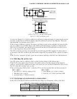
Figure 2.1.2.1 shows the external connection diagram.
V
DD
V
S1
V
L1
V
L2
V
L3
CA
CB
V
SS
3 V
Fig. 2.1.2.1 External connection in each LCD operation mode
For LCD driving, the internal voltage regulator generates the V
L1
voltage. The V
L2
and V
L3
voltage levels
are generated by boosting the V
L1
voltage.
The V
L1
voltage can be adjusted by feeding it back to the V
ADJ
pin through R
A1
and R
A2
as shown in
Figure 2.1.2.2. V
L
(
≈
V
DD
- V
L1
) is defined by following equation:
V
L
≈
1
×
(R
A1
+ R
A2
) / R
A1
Example:
V
L
≈
1 V
≈
1.5 V
R
A1
∞
2 M
Ω
R
A2
0
Ω
1 M
Ω
An LCD driving voltage suited to each
LCD panel can be obtained by adjusting
V
L
at the V
ADJ
pin.
R
A1
V
ADJ
V
L1
(1 M
Ω
)
(2 M
Ω
)
V
ADJ
V
L1
R
A2
Fig. 2.1.2.2 LCD voltage adjustment circuit


