


36
EPSON
E0C6006 TECHNICAL MANUAL
CHAPTER 4: PERIPHERAL CIRCUITS AND OPERATION (Remote Controller)
(2) Setting of carrier output width
In the soft-timer mode, the carrier output width (carrier output ON time) is controlled by writing to
the REMSO register, but in the hard-timer mode, it can be specified with values 0 to 3, which mean the
number of
τ
cycles described above, in each transmission data bit. Since the carrier output ON/OFF is
controlled by the hardware in synchronizing with
τ
waveform, it is unnecessary to watch the ON time
and to specify the OFF timing by the software.
The carrier output width can be selected by writing data to the ROUT1–ROUT0 register (F9H•D3, D2)
from among 4 types as shown in Table 4.9.4.3.
Table 4.9.4.3 Setting of carrier output width
Carrier output width
0
τ
1
τ
2
τ
3
τ
ROUT1
0
0
1
1
ROUT0
0
1
0
1
The carrier is output in synchronizing with the rising edge of the
τ
waveform after writing data to
ROUT register. Data written to the ROUT register is maintained while the REM circuit is ON until the
next data is written. The carrier output starts using the write signal for this register and the carrier
output will be ON from the rising edge of the
τ
waveform immediately after that until the period set
in the register has passed. In other words, the register data is valid only one time after writing.
Consequently, data must be written every time even when outputting the same data successively.
The ROUT register is set to "0H" at initial reset and when the REMC register is set to "0". Conse-
quently, after turning the REM circuit ON ("1" is written to the REMC register), REM output becomes
low level (V
SS
) until a value other than "0H" is written to the ROUT register.
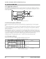
Figure 4.9.4.4 shows the timing of data writing to the ROUT register and the carrier output.
Register writing
ROUT1–0
τ
waveform
REMOUT
REM terminal
2
0
2
1
Fig. 4.9.4.4 Carrier output timing
Note: The values set in the ROUT register is taken into the REMOUT time generator synchronously with
the rise of a
τ
waveform. For this reason, avoid writing data into the ROUT register during one
carrier cycle immediately before and after the rise of the
τ
waveform.
(3) Remote controller (REM) interrupt
The carrier output ON time for one transmission data bit is controlled by writing data to the above
mentioned ROUT register. The OFF time is from when the output is turned OFF to when the next
carrier output starts by writing to the same register. Since the carrier output is turned ON at the rising
edge of the
τ
waveform after writing data, the next data must be written during the last
τ
cycle in the
carrier OFF period of the current transmission data. To decide its timing, an interrupt is used in the
hard-timer mode.
By using the interrupt, the CPU is released from the processing such as a timing watch, and can
execute other processing.
The timing to generate interrupt can be set by the software using
τ
cycle as reference the same as the
carrier output width. The interrupt timing can be selected by writing data to the RIC3–RIC0 register
(F8H).


