background image

8

EPSON

E0C6006 TECHNICAL MANUAL

CHAPTER 3: CPU, ROM, RAM

CHAPTER

 3 CPU, ROM, RAM

3.1 CPU

The E0C6006 employs the E0C6200B core CPU, so that register configuration, instructions, and so forth
are virtually identical to those in other processors in the family using the E0C6200/6200A/6200B. Refer to
the "E0C6200/6200A Core CPU Manual" for details of the E0C6200B.

Note the following points with regard to the E0C6006:

(1) The E0C6006 does not support the SLEEP function, therefore the SLP instruction cannot be used.

(2) Because the ROM capacity is 2,048 words, 12 bits per word, bank bits are unnecessary, and PCB and

NBP are not used.

(3) The RAM page is set to 0 only, so the page part (XP, YP) of the index register that specifies addresses is

invalid.
PUSH   XP       POP   XP       LD   XP,r       LD   r,XP
PUSH   YP       POP   YP       LD   YP,r       LD   r,YP

3.2 ROM

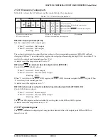
The built-in ROM, a mask ROM for the program, has a capacity of 2,048 

×

 12-bit steps. The program area

is 8 pages (0–7), each consisting of 256 steps (00H–FFH). After an initial reset, the program start address is
set to page 1, step 00H. The interrupt vectors are allocated to page 1, steps 01H–07H.

Step 00H

Step 07H

Step 08H

Step FFH

12 bits

Program start address

Interrupt vector area

Bank 0

Program area

Page 0

Page 1

Page 2

Page 3

Page 4

Page 5

Step 01H

Page 6

Page 7

Fig. 3.2.1  ROM configuration

3.3 RAM

The RAM, a data memory for storing a variety of data, has a capacity of 128 words, 4-bit words. When
programming, keep the following points in mind:

(1) Part of the data memory is used as stack area when saving subroutine return addresses and registers,

so be careful not to overlap the data area and stack area.

(2) Subroutine calls and interrupts take up three words on the stack.

(3) Data memory 000H–00FH is the memory area pointed by the register pointer (RP).

Содержание E0C6006

Страница 1: ...MF1114 01 CMOS 4 BIT SINGLE CHIP MICROCOMPUTER E0C6006 TECHNICAL MANUAL E0C6006 Technical Hardware ...

Страница 2: ...license to any intellectual property rights is granted by implication or otherwise and there is no representation or warranty that anything made in accordance with this material will be free from any patent or copyright infringement of a third party This material or portions thereof may contain technology or the subject relating to strategic products under the control of the Foreign Exchange and F...

Страница 3: ... 8 CHAPTER 4 PERIPHERAL CIRCUITS AND OPERATION__________________________ 9 4 1 Memory Map 9 4 2 Watchdog Timer 11 4 2 1 Configuration of watchdog timer 11 4 2 2 I O memory of watchdog timer 11 4 2 3 Programming note 11 4 3 Oscillation Circuit 12 4 3 1 Configuration of oscillation circuit 12 4 3 2 OSC1 oscillation circuit 12 4 3 3 OSC3 oscillation circuit 12 4 3 4 Switching the system clock 13 4 3 ...

Страница 4: ...nterrupt request 42 4 10 2 Interrupt mask register 44 4 10 3 Interrupt vector 44 4 10 4 Programming notes 45 4 11 Lower Current Dissipation 46 CHAPTER 5 BASIC EXTERNAL WIRING DIAGRAM ____________________________ 47 CHAPTER 6 ELECTRICAL CHARACTERISTICS ________________________________ 48 6 1 Absolute Maximum Rating 48 6 2 Recommended Operating Conditions 48 6 3 DC Characteristics 48 6 4 Analog Circ...

Страница 5: ...on Instruction execution time 32 kHz operation 153 214 or 366 µsec depending on instructions 455 kHz operation 11 15 or 26 µsec depending on instructions Instruction set 100 instructions Input port 8 ports with or without pull up resistor Output ports 4 ports clock and buzzer outputs are possible by mask option I O port 4 ports Infrared remote control output 1 output LCD driver 20 segments 3 or 4 ...

Страница 6: ...ESET P00 P03 R00 R01 R02 FOUT BZ 1 R03 BZ 1 R33 REM 1 Terminal specifications can be selected by mask option Core CPU E0C6200B ROM 2 048 words 12 bits System Reset Control Interrupt Generator RAM 128 words 4 bits LCD Driver 20 SEG 4 COM Power Controller OSC Clock Timer Watchdog Timer FOUT Buzzer Input Port I O Port Output Port REM Fig 1 2 1 E0C6006 block diagram ...

Страница 7: ... VS1 OSC2 OSC1 VDD P03 P02 P01 P00 N C No connection 31 45 16 30 INDEX 15 1 60 46 Fig 1 3 1 E0C6006 pin layout QFP6 60pin QFP13 64pin No 1 2 3 4 5 6 7 8 9 10 11 12 13 14 15 16 Pin name N C N C N C N C K00 K01 K02 K03 K10 K11 K12 K13 R00 R01 R02 R03 No 17 18 19 20 21 22 23 24 25 26 27 28 29 30 31 32 Pin name N C R33 REM SEG0 SEG1 SEG2 SEG3 SEG4 SEG5 SEG6 SEG7 SEG8 SEG9 SEG10 SEG11 N C TEST No 33 34...

Страница 8: ...put pin crystal Oscillation output pin crystal Oscillation input pin ceramic or CR Oscillation output pin ceramic or CR Input port pin Input port pin I O port pin Output port pin Output port pin BZ or FOUT output pin Output port pin or BZ output pin Remote control carrier output port pin LCD segment output pin or DC output pin LCD common output pin 1 3 duty or 1 4 duty are selectable Initial reset...

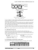
Страница 9: ...ed by the voltage regulator for stabilizing the oscillation 2 1 2 Voltage VL1 VL3 for LCD driving The on chip LCD voltage circuit generates the voltage levels VDD VL1 VL2 and VL3 needed to drive the LCD panel Figure 2 1 2 1 shows the external connection diagram VDD VS1 VL1 VL2 VL3 CA CB VSS 3 V Fig 2 1 2 1 External connection in each LCD operation mode For LCD driving the internal voltage regulato...

Страница 10: ...h level and the OSC1 oscillation circuit starts operating several milliseconds later the system is released from internal reset and starts to operate VDD OSC3 RESET Detect oscillation Watchdog timer Internal initial reset Vss GND Fig 2 2 1 1 Initial reset sequence at power on 2 2 2 RESET pin The RESET signal directly initializes the E0C6006 The system is reset when RESET L and released from the re...

Страница 11: ...ation frequency to perform the increment operation If the watchdog timer fails to be reset in 3 4 seconds with fOSC1 32 kHz the CPU will be initialized at initial reset See Section 4 2 Watchdog Timer for details 2 2 5 Initialization by initial reset When the E0C6006 is initially reset its internal registers are set as follows Table 2 2 5 1 Initial status See Section 4 1 Memory Map Name Program cou...

Страница 12: ...P YP LD YP r LD r YP 3 2 ROM The built in ROM a mask ROM for the program has a capacity of 2 048 12 bit steps The program area is 8 pages 0 7 each consisting of 256 steps 00H FFH After an initial reset the program start address is set to page 1 step 00H The interrupt vectors are allocated to page 1 steps 01H 07H Step 00H Step 07H Step 08H Step FFH 12 bits Program start address Interrupt vector are...

Страница 13: ... to display memory and 15 words to I O memory Figure 4 1 1 show the overall memory map for the E0C6006 and Table 4 1 1 the memory maps for the peripheral circuits I O space Address Page High Low 0 1 2 3 4 5 6 7 8 9 A B C D E F M0 M1 M2 M3 M4 M5 M6 M7 M8 M9 MA MB MC MD ME MF 3 0 1 2 4 5 6 7 8 9 A B C D E F 0 RAM area 000H 07FH 128 words 4 bits R W Display memory area 0D0H 0EFH 32 words 4 bits W onl...

Страница 14: ...1 TM10 0 0 0 0 Timer data 1 Hz Timer data 2 Hz Timer data 4 Hz Timer data 8 Hz 0F7H RCDIV RCDUTY RT1 RT0 R W RCDIV RCDUTY RT1 RT0 5 5 5 5 REM carrier interval and duty ratio setting τ cycle division ratio setting 0 1 12 1 1 16 2 1 20 3 1 32 0F2H REMC EIREM EIK1 EIK0 R W REMC EIREM EIK1 EIK0 1 0 0 0 On Enable Enable Enable Off Mask Mask Mask REM carrier generation on off Interrupt mask register REM...

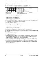
Страница 15: ...tus continues for 3 4 seconds the watch dog timer generates a CPU reset signal The watchdog timer function can be nullified by using the mask option 4 2 2 I O memory of watchdog timer Table 4 2 2 1 shows the I O address and control bit for the watchdog timer Table 4 2 2 1 Control bit of watchdog timer Address Comment D3 D2 Register D1 D0 Name Init 1 1 0 0F1H WDRST IT2 IT8 IT32 W R WDRST IT2 4 IT8 ...

Страница 16: ...llation frequency is 32 768 kHz Typ Figure 4 3 2 1 is the block diagram of the OSC1 oscillation circuit VDD VDD OSC2 OSC1 X tal CGX To CPU and peripheral circuits R FX CDX R DX Fig 4 3 2 1 OSC1 oscillation circuit crystal As shown in Figure 4 3 2 1 the crystal oscillation circuit can be configured simply by connecting the crystal oscillator X tal of 32 768 kHz Typ between the OSC1 and OSC2 termina...

Страница 17: ...C3 oscillation circuit should be stopped by the software OSCC register if unneces sary When Not Use is selected by mask option do not connect anything to the OSC3 and OSC4 terminals 4 3 4 Switching the system clock The CPU system clock is switched to OSC1 or OSC3 by the software CLKCHG register When OSC3 is to be used as the CPU clock it should be done as the following procedure using the software...

Страница 18: ...al reset this register is set to 1 CLKCHG CPU system clock switching register 0F6H D1 The CPU s operation clock is selected with this register When 1 is written OSC1 clock is selected When 0 is written OSC3 clock is selected Reading Valid When the CPU clock is to be OSC3 set CLKCHG to 0 for OSC1 set CLKCHG to 1 After turning the OSC3 oscillation ON OSCC 1 switching of the clock should be done afte...

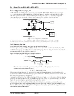
Страница 19: ...masked and the interrupt factor flags IK0 IK1 is set to 1 Input interrupt programming related precautions Factor flag is set Not set Mask register K port input Active status When the content of the mask register is rewritten while the port K input is in the active status The input interrupt factor flag is set at Fig 4 4 2 1 Input interrupt timing When using an input interrupt if you rewrite the co...

Страница 20: ... Interrupt mask register K10 K13 Interrupt mask register K00 K03 0F0H REMSO IREM IK1 IK0 R W R REMSO IREM 4 IK1 4 IK0 4 0 5 0 0 On Yes Yes Yes Off No No No Forced REM output on off Interrupt factor flag REM Interrupt factor flag K10 K13 Interrupt factor flag K00 K03 1 2 Initial value at initial reset Not set in the circuit 5 Undefined 3 4 Always 0 being read Reset 0 immediately after being read K0...

Страница 21: ...upt factor flag to be read is set to 1 an interrupt request will be generated by the interrupt factor flag set timing or an interrupt request will not be generated Be very careful when interrupt factor flags are in the same address At initial reset this flag is set to 0 4 4 5 Programming notes 1 When modifying the input port from low level to high level with pull up resistor a delay will occur at ...

Страница 22: ... mode the output terminal goes high VDD when 1 is written to the data register and goes low VSS when 0 is written At initial reset the output terminal goes low 4 5 2 Mask option The mask option enables the following output port selection 1 Output specifications of output ports The output specifications for the output port R00 R03 can be selected from complementary output and Nch open drain output ...

Страница 23: ...02 will output the clock generated from the OSC1 oscillation clock fOSC1 The clock frequency can be selected from among 8 types by mask option Table 4 5 3 1 FOUT clock frequency Dividing ratio fOSC1 fOSC1 2 fOSC1 4 fOSC1 8 fOSC1 16 fOSC1 32 fOSC1 64 fOSC1 128 Frequency 32768 Hz 16384 Hz 8192 Hz 4096 Hz 2048 Hz 1024 Hz 512 Hz 256 Hz No 1 2 3 4 5 6 7 8 When fOSC1 32 768 kHz When 1 is written to the ...

Страница 24: ... is written the terminals go low Figure 4 5 3 3 shows the buzzer direct drive waveform R03 R02 register BZ output waveform BZ output waveform 0 1 0 Fig 4 5 3 3 Buzzer output waveform direct driving Single terminal driving of piezo electric buzzer The piezo electric buzzer can be driven with one terminal by setting the R03 to the BZ output terminal At initial reset the BZ output goes off and the ou...

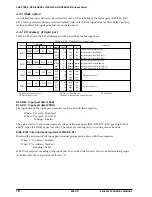
Страница 25: ...e output port terminals output the data written to the corresponding registers R00 R03 without changing it When 1 is written to the register the output port terminal goes high VDD and when 0 is written the output port terminal goes low VSS At initial reset these registers are all set to 0 R02 when FOUT is selected Special output control 0FCH D2 Controls the FOUT clock output When 1 is written Cloc...

Страница 26: ...during read operation The output mode is set when 1 is written to the I O control register IOC When the I O ports are set to the output mode they work as output ports and output a high signal VDD when the port output data is 1 and a low signal VSS when the port output data is 0 If perform the read out in each mode when output mode the register value is read out and when input mode the port value i...

Страница 27: ...rt terminals are pulled up IOC I O control register 0FFH D1 The input or output mode can be set with this register When 1 is written Output mode When 0 is written Input mode Reading Valid When 1 is written to the I O control register the I O ports enter the output mode and when 0 is written the I O ports enter the input mode At initial reset this register is set to 0 4 6 4 Programming notes 1 When...

Страница 28: ... power for driving the LCD is generated by the internal circuit so that there is no need to apply power especially from outside The frame frequency is 32 Hz for 1 4 duty and 42 7 Hz for 1 3 duty in the case of fOSC1 32 768 kHz Figures 4 7 1 1 and 4 7 1 2 show the drive waveform for 1 3 duty and 1 4 duty Table 4 7 1 1 LCD drive mode options Duty 1 4 1 3 COM used COM0 COM3 COM0 COM2 Max number of se...

Страница 29: ... 25 CHAPTER 4 PERIPHERAL CIRCUITS AND OPERATION LCD Driver COM0 COM1 COM2 COM3 V V V V DD L1 L2 L3 V V V V DD L1 L2 L3 SEG0 SEG19 Frame frequency Off On LCD status COM0 COM1 COM2 COM3 SEG0 19 Fig 4 7 1 2 Drive waveform for 1 4 duty ...

Страница 30: ...an example of the relationship between the LCD segments on the panel and the display memory in the case of 1 3 duty a a f f g g e e d d p p c b b c SEG10 SEG11 SEG12 Common 0 Common 1 Common 2 0ECH 0EDH 0EEH 0EFH Address d p d p D3 c g c g D2 b f b f D1 a e a e D0 Data Display memory allocation SEG10 SEG11 SEG12 EC D0 a EC D1 b EF D1 f ED D1 f ED D2 g EC D2 c ED D0 e EC D3 d ED D3 p Pin address al...

Страница 31: ...her frequency at OSC1 substitute the appropriate value for 32 768 kHz throughout this section 4 8 2 Interrupt function The clock timer can generate interrupts at the falling edge of the 32 Hz 8 Hz and 2 Hz signals The software can mask any of these interrupt signals Figure 4 8 2 1 is the timing chart of the clock timer Address 0F4H 0F5H 32 Hz interrupt request 8 Hz interrupt request 2 Hz interrupt...

Страница 32: ...er 8 Hz Interrupt factor flag clock timer 32 Hz 1 2 Initial value at initial reset Not set in the circuit 5 Undefined 3 4 Always 0 being read Reset 0 immediately after being read TM00 TM03 Timer low order data 0F4H TM10 TM13 Timer high order data 0F5H The l28 Hz to 16 Hz timer data of the clock timer can be read from the TM00 TM03 register and 8 Hz to 1 Hz data can be read from the TM10 TM13 regis...

Страница 33: ...ul in the following cases If the interrupt mask register value corresponding to the interrupt factor flag to be read is set to 1 an interrupt request will be generated by the interrupt factor flag set timing or an interrupt request will not be generated Be very careful when interrupt factor flags are in the same address At initial reset these flags are set to 0 4 8 4 Programming notes 1 Note that ...

Страница 34: ...nfrared remote controllers employ a method that generates transmission waveforms in pulse modulation as shown in Figure 4 9 1 3 and transmits the signal First the transmission code is modulated in a pulse phase modulation PPM method to generate the modulation signal and the carrier that has constant frequency is amplitude modulated AM using the modulation signal As a result transmission waveforms ...

Страница 35: ...ths Fixed to several cycles Stabilized at setting Hard timer mode Difficult Source oscillation sway and errors caused by instruction cycles Variable to any width Variable Duty slightly disturbed before and after ON time Soft timer mode 4 9 2 Carrier The carrier is generated by the carrier generation circuit using the OSC3 clock as the source clock Note If an option is selected without use of OSC3 ...

Страница 36: ...ore waiting time for oscillation stabilization after turning the OSC3 oscillation ON Further the oscillation stabilization time varies depending on the external oscillator characteristics and conditions of use so allow ample margin when setting the waiting time Figure 4 9 2 1 shows the carrier waveform OSC3 clock 1 8 division 1 4 duty 1 8 division 3 8 duty 1 12 division 1 3 duty 1 12 division 1 4 ...

Страница 37: ...d when 0 is written the REM terminal goes low level VSS However the carrier must be generated by writing 1 to the REMC register before writing 1 to the REMSO register Figure 4 9 3 2 shows the timing chart in the soft timer mode REMC register Carrier REMSO register REM R33 output Fig 4 9 3 2 Timing chart soft timer mode Note Writing to the REMSO register without synchronization with the carrier gen...

Страница 38: ... to the REMSO register REM output are forcibly done regardless of the control of the hard timer mode 1 τ reference cycle τ reference cycle is used as reference for the carrier output ON time and interrupt timing specified by the software and is generated by the τ reference cycle generation circuit by dividing carrier This dividing ratio can be selected using the RT1 RT0 register F7H D1 D0 from 4 t...

Страница 39: ... 4 9 4 2 REMC Carrier τ waveform Stop synchronously with τ Fig 4 9 4 2 REM circuit stop timing Maximum of 384 machine cycles are required until the REM circuit stops after the REMC is set to 0 Even if the CPU clock is changed from OSC3 to OSC1 after the REMC 0 OSC3 must not be turned OFF before the REM circuit stops This time depends on the value of the set τ cycle If a shorter τ cycle is set the ...

Страница 40: ...successively The ROUT register is set to 0H at initial reset and when the REMC register is set to 0 Conse quently after turning the REM circuit ON 1 is written to the REMC register REM output becomes low level VSS until a value other than 0H is written to the ROUT register Figure 4 9 4 4 shows the timing of data writing to the ROUT register and the carrier output Register writing ROUT1 0 τ wavefor...

Страница 41: ...H D2 However regardless of the setting of the interrupt mask register the interrupt factor flag IREM is set to 1 when the counting of the interrupt τ cycles are completed The interrupt factor flag is reset to 0 by the reading Data written to the RIC register is maintained while the REM circuit is ON until the next data is written However the counting of τ waveform starts using the write signal for...

Страница 42: ...e circuit 5 Undefined 3 4 Always 0 being read Reset 0 immediately after being read D3 0 0 1 1 D2 0 1 0 1 Div ratio 1 8 1 8 1 12 1 12 Duty 1 4 3 8 1 3 1 4 REMC REM carrier generation control 0F2H D3 Turns the carrier generation on and off When 1 is written On When 0 is written Off Reading Valid When 1 is written to the REMC register the carrier generation circuit turns ON Writing 0 turns the carrie...

Страница 43: ... 5 4 Setting of carrier output width Carrier output width 0τ 1τ 2τ 3τ ROUT1 0 0 1 1 ROUT0 0 1 0 1 By writing data to this register the carrier for set τ cycles is output from the REM R33 terminal in synchronization with the rising edge of the τ waveform immediately after that The setting writing of carrier output width must be done at every bit of the transmission data At initial reset and when th...

Страница 44: ... not occurred Writing Invalid This flag is set to 1 when the interrupt τ cycle set with the RIC register has passed counting of the τ waveform has completed From the status of this flag the software can decide the remote controller interrupt Note however that even if the interrupt is masked this flag will be set to 1 when the counting of the interrupt τ cycle is completed This flag is reset when r...

Страница 45: ... during which OSC3 must be held ON 4 With the REM circuit in operation do not write data at addresses 0F8H and 0F9H REM interrupt counter and REMOUT time setting register during an interval of one carrier before and after the rise of τ 5 With the REM circuit in operation do not write data at addresses 0F7H τ setting register 6 During the operation under hard timer mode the REMSO register must be f...

Страница 46: ...0 Run Enable Enable Enable Reset Stop Mask Mask Mask Timer run reset stop Interrupt mask register clock timer 2 Hz Interrupt mask register clock timer 8 Hz Interrupt mask register clock timer 32 Hz 0F1H WDRST IT2 IT8 IT32 W R WDRST IT2 4 IT8 4 IT32 4 Reset 0 0 0 Reset Yes Yes Yes No No No Watchdog timer reset Interrupt factor flag clock timer 2 Hz Interrupt factor flag clock timer 8 Hz Interrupt f...

Страница 47: ... OSC3 Input Interrupt An input interrupt can be invoked by the IK1 group K10 K13 or the IK0 group K00 K03 As each pin contains an fOSC1 8 4 kHz clock noise reject circuit the input must be held at low level for at least 16 fOSC1 0 5 msec to assure an input interrupt For the K10 K13 group the interrupt factor flag can be set with the noise reject circuit bypassed by using the mask option In this ca...

Страница 48: ...errupt mask register One interrupt mask register is available to each interrupt factor flag to mask an interrupt request Data can be written to or read from the mask register An interrupt request is enabled with 1 set in the register and masked with 0 set in the register At initial reset the mask register is reset to 0 Table 4 10 2 1 Interrupt mask register Interrupt mask register ETI2 ETI8 ETI32 ...

Страница 49: ...ate at the beginning of the interrupt processing routine 3 The interrupt factor flags must always be reset before setting the EI status When the interrupt mask register has been set to 1 the same interrupt will occur again if the EI status is set unless of resetting the interrupt factor flag 4 The interrupt factor flag will be reset by reading through the software Because of this when multiple int...

Страница 50: ...k timer Control register HALT instruction CLKCHG OSCC REMC TMRUN Order of current consumption See Capter 6 Electrical Characteristics Several tens µA Several µA in OSC3 mode Several hundreds nA OSC3 not used selected Several hundreds nA At initial setting with the CPU in operation mode the CPU is ready with OSC3 clock CLKCHG 0 in high speed mode the ceramic CR oscillation circuit is ON OSCC 1 the ...

Страница 51: ...REM R02 R03 P00 P03 K00 K03 K10 K13 R00 R01 Vss VDD E0C6006 SR C SR S GX C CL1 CL2 CL3 GC C DC C S1 C A2 R A1 R D RB RRC X tal CGX CR CGC CDC CSR RA1 RA2 RA3 RA4 C1 CS1 CL1 CL3 Crystal oscillator Trimmer capacitor Ceramic oscillator Capacitor Capasitor Capacitor Resistor Resistor Resistor Capacitor Capacitor Capacitor 32 768kHz CI Max 35kΩ 5 25pF 455kHz 100pF 100pF 0 33µF Open VL 1 0V 2MΩ VL 1 5V ...

Страница 52: ...tage 2 High level input current Low level input current High level output current 1 Low level output current 1 High level output current 2 Low level output current 2 High level output current 3 Low level output current 3 Common output current Segment output current during LCD output 1 Unless otherwise specified VDD 0V VSS 2 2 to 3 5V VL3 3 0V Ta 20 to 70 C Symbol VIH1 VIL1 VIH2 VIL2 IIH IIL1 IIL2 ...

Страница 53: ...in Frequency voltage deviation Frequency IC deviation Frequency adjustment range Harmonic oscillation start voltage Permitted leak resistance Symbol tsta CD f V f IC f CG Vhho Rleak Unit sec pF pF ppm ppm ppm V MΩ Max 3 5 10 3 5 Typ 20 19 Min 10 40 200 Condition VSS 2 2 to 3 5V Package as assembled Bare chip VSS 2 2 to 3 5V CG 5 to 25pF CG 5pF VSS Between OSC1 and other pins Unless otherwise speci...

Страница 54: ...board and package capacitance Note Oscillation characteristics are affected by various conditions board pattern parts used etc 100 30 50 100 500 1000 f OSC3 kHz 500 1000 R k CR Ω TYP 200 200 6 6 Input Current Characteristics For Reference Condition Ta 25 C VDD 0 V VSS 3 0 V RESET P 0 0 10 20 1 2 3 VIH V I IH µA 0 0 2 4 6 1 2 3 VIH V I IH µA K 0 0 4 8 12 1 2 3 VIH V I IH µA ...

Страница 55: ...ut Current Characteristics For Reference Condition Ta 25 C VDD 0 V R0 P R0 P Vss 0 10 20 30 Vss 1 Vss 2 Vss 3 VOL V I OL mA Vss 2 2 V Vss 3 0 V P0 R0 P0 R0 0 0 2 4 6 8 1 2 3 VOH V I OH mA Vss 2 2 V Vss 3 0 V P0 R0 P0 R0 R33 REM 0 0 10 20 30 1 2 3 VOH V I OH mA Vss 2 2 V Vss 3 0 V ...

Страница 56: ... 17 6 0 4 31 45 14 0 2 17 6 0 4 16 30 INDEX 0 35 0 1 15 1 60 46 2 7 0 1 0 1 3 1 max 1 8 0 85 0 2 0 10 0 15 0 05 0 8 QFP13 64pin Unit mm 10 0 1 12 0 4 33 48 10 0 1 12 0 4 17 32 INDEX 0 18 16 1 64 49 1 4 0 1 0 1 1 7 max 1 0 5 0 2 0 10 0 125 0 1 0 05 0 05 0 025 0 5 The dimensions are subjected to change without notice ...

Страница 57: ... VADJ CA CB VSS OSC4 OSC3 VS1 No 17 18 19 20 21 22 23 24 25 26 27 28 29 30 31 32 Pin name OSC2 OSC1 VDD P03 P02 P01 P00 N C N C N C K00 K01 K02 K03 K10 K11 No 33 34 35 36 37 38 39 40 41 42 43 44 45 46 47 48 Pin name K12 K13 R00 R01 R02 R03 N C N C N C R33 REM SEG0 SEG1 SEG2 SEG3 SEG4 SEG5 No 49 50 51 52 53 54 55 56 57 58 59 60 61 62 63 64 Pin name SEG6 SEG7 SEG8 SEG9 SEG10 SEG11 N C TEST RESET SEG...

Страница 58: ... 28 29 30 31 32 33 34 35 36 37 38 Pad name SEG16 SEG17 SEG18 SEG19 COM3 COM2 COM1 COM0 VL1 VL2 VL3 VADJ CA CB VSS OSC4 OSC3 VS1 OSC2 X 1204 1204 1204 1204 1204 1204 1204 1204 1204 1204 1204 1184 997 867 130 0 130 260 390 Y 338 208 78 52 236 366 496 626 756 886 1024 1285 1285 1285 1285 1285 1285 1285 1285 No 39 40 41 42 43 44 45 46 47 48 49 50 51 52 53 54 55 56 Pad name OSC1 VDD P03 P02 P01 P00 K00...

Страница 59: ...OSC2 OSC1 VDD OSC4 OSC3 VDD In order to prevent unstable operation of the oscillation circuit due to current leak between OSC1 OSC3 and VSS please keep enough distance between OSC1 OSC3 and VSS or other signals on the board pattern Reset Circuit The power on reset signal which is input to the RESET terminal changes depending on conditions power rise time components used board pattern etc Decide th...

Страница 60: ...tance or intersects a high speed line noise may generated by mutual interference between the signals and it may cause a malfunction Do not arrange a high speed signal line especially near circuits that are sensitive to noise such as the oscillation unit Prohibited pattern OSC4 OSC3 VDD Large current signal line High speed signal line Precautions for Visible Radiation when bare chip is mounted Visi...

Страница 61: ...one 33 0 1 64862350 Fax 33 0 1 64862355 ASIA HONG KONG CHINA EPSON HONG KONG LTD 20 F Harbour Centre 25 Harbour Road Wanchai HONG KONG Phone 852 2585 4600 Fax 852 2827 4346 Telex 65542 EPSCO HX CHINA SHANGHAI EPSON ELECTRONICS CO LTD 4F Bldg 27 No 69 Gui Jing Road Caohejing Shanghai CHINA Phone 21 6485 5552 Fax 21 6485 0775 TAIWAN R O C EPSON TAIWAN TECHNOLOGY TRADING LTD 10F No 287 Nanking East R...

Страница 62: ...ursuit of Saving Technology Epson electronic devices Our lineup of semiconductors liquid crystal displays and quartz devices assists in creating the products of our customers dreams Epson IS energy savings ...

Страница 63: ...ELECTRONIC DEVICES MARKETING DIVISION Electronic devices information on the Epson WWW server http www epson co jp Issue SEPTEMBER 1998 Printed in Japan M A ...

Отзывы: