72
4317I–AVR–01/08
AT90PWM2/3/2B/3B
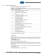
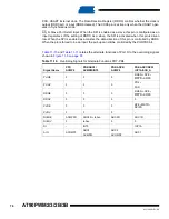
ADC10, Analog to Digital Converter, input channel 10.
ACMP1, Analog Comparator 1 Positive Input. Configure the port pin as input with the internal
pull-up switched off to avoid the digital port function from interfering with the function of the Ana-
log Comparator.
• ADC9/AMP1+ – Bit 5
ADC9, Analog to Digital Converter, input channel 9.
AMP1+, Analog Differential Amplifier 1 Positive Input Channel.
• ADC8/AMP1- – Bit 4
ADC8, Analog to Digital Converter, input channel 8.
AMP1-, Analog Differential Amplifier 1 Negative Input Channel.
• T1/PSCOUT23 – Bit 3
T1, Timer/Counter1 counter source.
PSCOUT23: Output 3 of PSC 2.
• T0/PSCOUT22 – Bit 2
T0, Timer/Counter0 counter source.
PSCOUT22: Output 2 of PSC 2.
• PSCIN1/OC1B, Bit 1
PCSIN1, PSC 1 Digital Input.
OC1B, Output Compare Match B output: This pin can serve as an external output for the
Timer/Counter1 Output Compare B. The pin has to be configured as an output (DDC1 set “one”)
to serve this function. This pin is also the output pin for the PWM mode timer function.
• PSCOUT10/INT3 – Bit 0
PSCOUT10: Output 0 of PSC 1.
INT3, External Interrupt source 3: This pin can serve as an external interrupt source to the MCU.
Содержание AT90PWM2
Страница 344: ...346 4317I AVR 01 08 AT90PWM2 3 2B 3B 31 1 SO24...
Страница 345: ...347 4317I AVR 01 08 AT90PWM2 3 2B 3B 31 2 SO32...
Страница 346: ...348 4317I AVR 01 08 AT90PWM2 3 2B 3B 31 3 QFN32...
Страница 347: ...349 4317I AVR 01 08 AT90PWM2 3 2B 3B...


