151
4317I–AVR–01/08
AT90PWM2/3/2B/3B
16.11 PSC Input Mode 3: Stop signal, Execute Opposite while Fault active
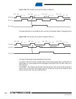
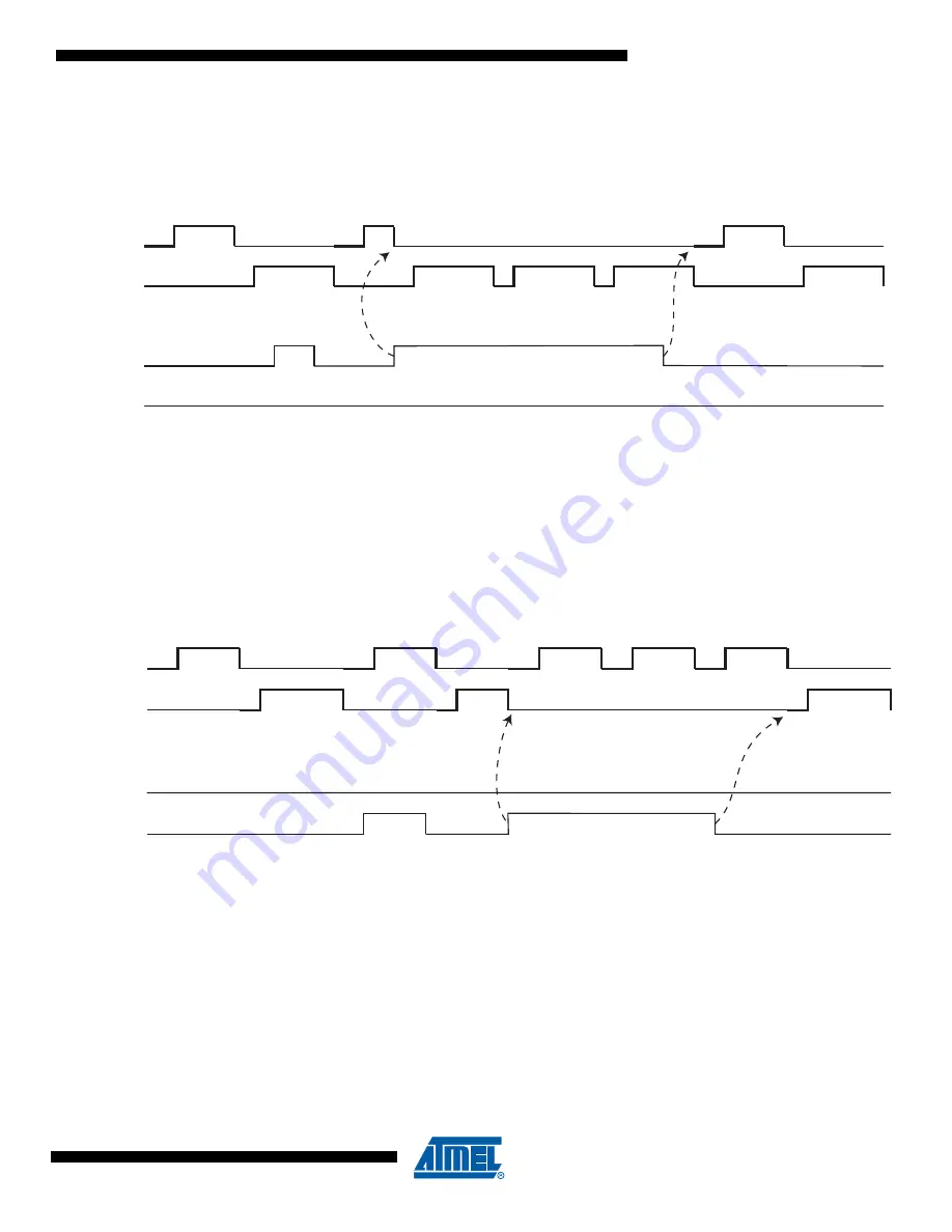
Figure 16-24. PSCn behaviour versus PSCn Input A in Mode 3
PSC Input A is taken into account during DT0 and OT0 only. It has no effect during DT1 and
OT1.
When PSC Input A event occurs, PSC releases PSCOUTn0, jumps and executes DT1 plus OT1
plus DT0 while PSC Input A is in active state.
Even if PSC Input A is released during DT1 or OT1, DT1 plus OT1 sub-cycle is always com-
pletely executed.
Figure 16-25. PSCn behaviour versus PSCn Input B in Mode 3
PSC Input B is taken into account during DT1 and OT1 only. It has no effect during DT0 and
OT0.
When PSC Input B event occurs, PSC releases PSCnOUT1, jumps and executes DT0 plus OT0
plus DT1 while PSC Input B is in active state.
Even if PSC Input B is released during DT0 or OT0, DT0 plus OT0 sub-cycle is always com-
pletely executed.
16.12 PSC Input Mode 4: Deactivate outputs without changing timing.
PSCOUTn0
PSCOUTn1
PSC Input A
PSC Input B
DT0
OT0
DT1
OT1
DT0 OT0 DT1
OT1
DT0
OT0
DT1
OT1
DT1
OT1
DT1
OT1
PSCOUTn0
PSCOUTn1
PSC Input A
PSC Input B
DT0
OT0
DT1
OT1
DT0
OT0
DT1
OT1
DT0
OT0
DT1
OT1
DT0
OT0
DT0
OT0
Содержание AT90PWM2
Страница 344: ...346 4317I AVR 01 08 AT90PWM2 3 2B 3B 31 1 SO24...
Страница 345: ...347 4317I AVR 01 08 AT90PWM2 3 2B 3B 31 2 SO32...
Страница 346: ...348 4317I AVR 01 08 AT90PWM2 3 2B 3B 31 3 QFN32...
Страница 347: ...349 4317I AVR 01 08 AT90PWM2 3 2B 3B...

