


System Overview
3-16
hardware flow control is enabled for the port (FC bit in the serial port 0
control register is set). The RTR0 signal is asserted when the associated
serial port receive register does not contain valid, unread data.
RXD0/PIO23
Receive Data 0 (input, asynchronous)
This pin supplies asynchronous serial receive data from the system to
asynchronous serial port 0.
RXD1/PIO28
Receive Data 1 (input, asynchronous)
This pin supplies asynchronous serial receive data from the system to
asynchronous serial port 1.
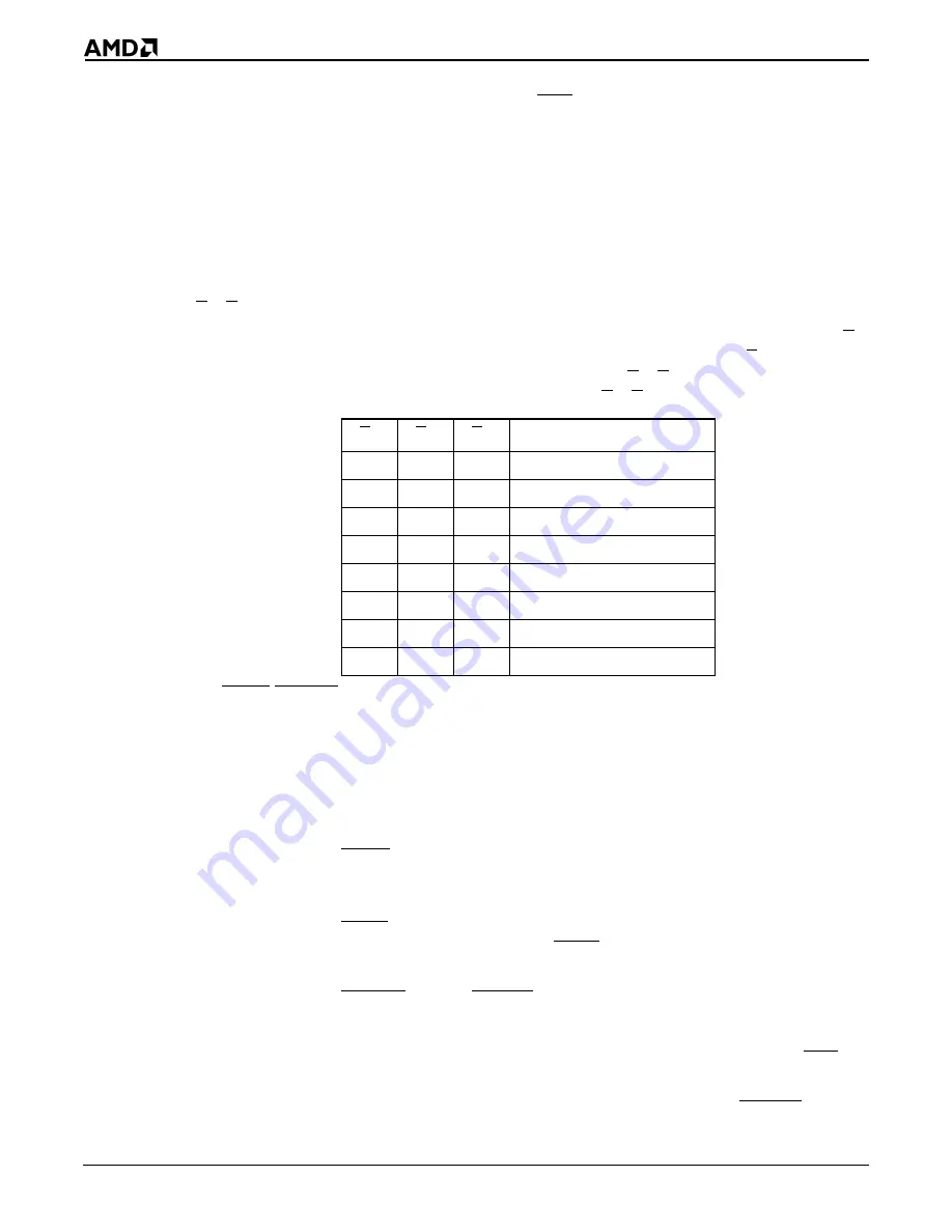
S2–S0
Bus Cycle Status (output, three-state, synchronous)
These pins indicate to the system the type of bus cycle in progress. S2
can be used as a logical memory or I/O indicator, and S1 can be used
as a data transmit or receive indicator. S2–S0 float during bus hold and
hold acknowledge conditions. The S2–S0 pins are encoded as shown.
S6/LOCK/CLKDIV2/PIO29
Bus Cycle Status Bit 6 (output, synchronous)
Bus Lock (output, synchronous)
Clock Divide by 2 (input, internal pullup)
S6—During the second and remaining periods of a cycle (t
2
, t
3
, and t
4
),
this pin is asserted High to indicate a DMA-initiated bus cycle. During
a bus hold or reset condition, S6 floats.
LOCK—This signal is asserted Low to indicate to other system bus
masters that they are not to gain control of the system bus. This signal
is only available during t
1
.
LOCK on the Am186ES and Am188ES microcontrollers does not
conform to the timing of the LOCK signal on the 80C186/188
microcontrollers. This signal is primarily intended for use by emulators.
CLKDIV2—If S6/CLKDIV2/PIO29 is held Low during power-on reset,
the chip enters clock divided by 2 mode where the processor clock is
derived by dividing the external clock input by 2. If this mode is selected,
the PLL is disabled. The pin is sampled on the rising edge of RES.
If S6 is to be used as PIO29 in input mode, the device driving PIO29
must not drive the pin Low during power-on reset. S6/CLKDIV2/PIO29
S2
S1
S0
Bus Cycle
0
0
0
Interrupt acknowledge
0
0
1
Read data from I/O
0
1
0
Write data to I/O
0
1
1
Halt
1
0
0
Instruction fetch
1
0
1
Read data from memory
1
1
0
Write data to memory
1
1
1
None (passive)
Содержание Am186 ES
Страница 1: ...Am186 ES and Am188 ES User s Manual...
Страница 4: ...iv...
Страница 12: ...Table of Contents xii...
Страница 22: ...Features and Performance 1 8...
Страница 60: ...System Overview 3 28...
Страница 84: ...Chip Select Unit 5 14...
Страница 132: ...Timer Control Unit 8 8...
Страница 166: ...Programmable I O Pins 11 6...
Страница 184: ...Register Summary A 18...