background image

Stratix II Memory Board 2 Rev A User Guide Rev 0.1 


Altera Confidential 

16


The DDR2 SDRAM Devices test uses a hardware state machine included in the DDR2 

MegaCore® function, and a DDR2 SDRAM Devices to test the DDR2 interface. For 

further details on this test, refer to “DDR2 SDRAM Devices Test” in section 3.3.3. 

2.3.4.1


Required Hardware 

1.  The board has been tested with the following DDR2 SDRAM devices, and is expected 

to be compatible with other industry standard DDR2 SDRAM devices. 


• Micron Technology MT47H16M16BG - 37B 

• Samsung Semiconductor K4H561638F-TCCC 


2.3.4.2


Test Setup 

Perform the following steps to set up the DDR2 SDRAM Devices test. 


1. Move the power switch to the OFF position. 


2. Set the switches (MPGM pins) on S1 to the correct values for this test, as shown in 

Table 2.


3. Move the power switch to the ON position. 


4. Press the SYS_RESETn (S3) pushbutton to reload the FPGA. 


5. Confirm that the Stratix II device has finished configuration (the CONF_DONEn LED 

(D12) illuminates).  The Error LED (D17) will illuminate if there is an error. 


2.3.4.3


Run the DDR2 SDRAM Devices Test 

Perform the following steps to execute the DDR2 SDRAM Devices test. 


1. Press the PB3 (S8) pushbutton to reset and run the design. 


2. Confirm that LED0 and LED1 are on, and that LED4 and LED5 are blinking. If so, the 

test is a success. LED0 turns on to indicate that the test is not failing.  LED1 turns on to 

indicate that the test is complete. 


2.3.5


QDRII SRAM Device(s) Test 

For further details on this test, refer to “QDRII SRAM Device(s) Test” in section 3.3.4. 

2.3.5.1


Test Setup 

Perform the following steps to set up the QDRII SRAM Device(s) test. 


1. Move the power switch to the OFF position. 

Содержание Stratix II

Страница 1: ...Stratix II Memory Board 2 Rev A User Guide Rev 0 1 Altera Confidential 1 Stratix II Memory Board 2 Rev A User Guide Rev 0 1 High Speed End Applications Team Wednesday November 03 2004 ...

Страница 2: ...cts are protected under numerous U S and foreign patents and pending applications maskwork rights and copyrights Altera warrants performance of its semiconductor products to current specifications in accordance with Altera s standard warranty but reserves the right to make changes to any products and services at any time without notice Altera assumes no responsibility or liability arising out of t...

Страница 3: ...Diagnostic Tests 10 2 3 1 User I O Test 11 2 3 2 Nios Stamp Features Test 12 2 3 3 DDR2 SDRAM DIMM Test 14 2 3 4 DDR2 SDRAM Devices Test 15 2 3 5 QDRII SRAM Device s Test 16 3 Diagnostic Tests 17 3 1 Set up S2MB2 for Individual Diagnostic Tests 17 3 1 1 Set up the Board 18 3 1 2 Power up Procedure 20 3 1 3 Running All Tests at Once 20 3 1 4 User IO Test 20 3 1 5 NIOS Stamp Features Test 21 3 1 6 D...

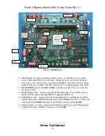
Страница 4: ...showcase high speed memories DDR2 SDRAM and QDRII SRAM with Altera s current high end device Stratix II using Altera developed Intellectual Property IP The main function of this board is to provide in house hardware verification and demonstration platforms for the Stratix II DDR2 SDRAM DIMM DDR2 SDRAM devices and QDRII SRAM memory controller IP The S2MB2 is shown in Figure 1 For detailed informati...

Страница 5: ...s which can be used to demonstrate DDR2 SDRAM DIMM interface at 267 MHz DDR2 SDRAM device interface at 267 MHz and QDRII device interface at 250 MHz Compact Discs CDs The S2MB2 includes CDs that contain the Quartus II design software including a one year evaluation license the MegaCore IP Library including OpenCore Plus free evaluation the Nios II embedded processor the board design files demonstr...

Страница 6: ...uld also verify that your computer meets the software and system requirements of the board 2 1 1 Development Board Contents The Stratix II Memory Board 2 contains the following items Stratix II Memory Board 2 USB Blaster download cable Power supply S2MB2 Stratix II Edition CD ROM MegaCore IP Library CD ROM Nios II CD ROM Quartus II Development Software CD ROM version 4 1 service pack 2 Stratix II ...

Страница 7: ... interface It must have a resistor value modified before the card is connected to a powered up S2MB2 or the resistor will overheat and fail The resistor is R8 The new value needs to be approximately 4 5k Ohms Ethernet connection w cable An Ethernet connection and cable is required to verify the Ethernet port on the S2MB2 As the test is currently configured the S2MB2 attempts to use DHCP to acquire...

Страница 8: ...ct the path of the folder into which you wish to restore the contents of the QAR File or select a folder with Browse 4 Click Show log to view the Quartus II Archive Log File qarlog for the project you are restoring from the QAR File 5 Click OK 2 1 6 Set Unused Pins in Your Design When compiling designs Altera recommends that all unused pins act as tri stated inputs To change this setting in the Qu...

Страница 9: ...tratix II Memory Board 2 Run the Preloaded Diagnostic Tests in section 2 3 describes how to set up and run each preloaded design and the required equipment Set up S2MB2 for Individual Diagnostic Tests in section 3 1 explains how to run the production tests Troubleshooting in section 3 2 describes how to solve problems you may encounter with the test designs or with setting up the board Diagnostic ...

Страница 10: ...ests are not exhaustive they help you confirm that each interface runs according to its intended design A subset of the diagnostic tests are loaded into the Stratix II Memory Board 2 s Flash memory If the S2MB2 does have preloaded diagnostic tests already in Flash then at power up the MAX or MAX II device checks the MPGM value and uses the Flash memory to configure the Stratix II device with the d...

Страница 11: ... In addition to your board you need the following hardware and software to perform this test Quartus II 4 1 SP2 or later software Board test system BTS files RS 232 cable 2 3 1 2 Test Setup Perform the following steps to set up the user I O test 1 Move the power switch to the OFF position 2 Connect one end of the RS 232 cable to port A J12 of the board and the other end of the cable to the COM1 po...

Страница 12: ...n Observe the corresponding switch indicator in the GUI b Set all of the dipswitches to the closed position Observe the corresponding switch indicator in the GUI 7 Test the User pushbuttons a Press the S5 S6 and S7 PB0 PB1 PB2 pushbuttons Observe the status in the GUI Do not press the S3 SYS_RESETn or S8 PB3 pushbuttons as these will reset the system If you accidentally press either of these butto...

Страница 13: ... downloads the required Nios code to the FPGA and launches the BTS GUI Wait for the BTS GUI to open If there is an error in the setup the BTS GUI will not start Please make sure that only one bts_test bat is running at a time 2 3 2 3 Run the Nios Stamp Test Perform the following steps to execute the Nios Stamp test 1 Choose Open Port RS232 Com1 BTS menu to open the COM1 port 2 Click the Nios Stamp...

Страница 14: ...ess returned may be different from the example above 8 Click the Blink Ethernet LEDs button 9 Verify that the LEDs on the Ethernet connector blink several times 10 If the Stratix II high speed development board is not connected to a live network the Ethernet tests cannot work correctly In this case look for the following message in the BTS message window in the bottom of the GUI It takes about 1 m...

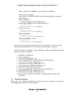
Страница 15: ...orm the following steps to set up the DDR2 SDRAM DIMM test 1 Move the power switch to the OFF position 2 Insert the DDR2 DIMM into J15 3 Set the switches MPGM pins on S1 to the correct values for this test as shown in Table 2 4 Move the power switch to the ON position 5 Press the SYS_RESETn S3 pushbutton to reload the FPGA 6 Confirm that the Stratix II device has finished configuration the CONF_DO...

Страница 16: ...he correct values for this test as shown in Table 2 3 Move the power switch to the ON position 4 Press the SYS_RESETn S3 pushbutton to reload the FPGA 5 Confirm that the Stratix II device has finished configuration the CONF_DONEn LED D12 illuminates The Error LED D17 will illuminate if there is an error 2 3 4 3 Run the DDR2 SDRAM Devices Test Perform the following steps to execute the DDR2 SDRAM D...

Страница 17: ...p functions are exercised using a prototype of the Board Test System BTS This design is the safe image that is loaded by pressing the SAFE button S2 This loads a NIOS based system design that will communicate with the host using a RS232 link The user interface is TCL based The GUI has several pages for the various features that are tested The memory tests are hardware based at this point and are s...

Страница 18: ...r Set up the DIP switches as shown in Table 3 Set up the S2MB2 jumpers as shown in Table 5 Table 3 DIP Switch Settings DIP Switch Name Setting S1 8 MSEL3 Open S1 7 MSEL2 Closed S1 6 MSEL1 Open S1 5 MSEL0 Open S1 4 RU_N_LU Open S1 3 MPGM2 Closed S1 2 MPGM1 Closed S1 1 MPGM0 Closed S4 1 to 8 USER DIP 0 7 Closed Open logic 1 Closed logic 0 Table 4 Other Switch Settings SW1 POWER OFF Table 5 Jumper Se...

Страница 19: ... the DDR2 DIMM carefully if needed Try not to flex the board if possible RS232 Serial Cable Connect one end of the serial cable to the COM 1 port on the PC and the other to the upper RS232 connector RS232 A USB Blaster cable Connect one end of the USB cable to a USB port on the PC and the other end to the USB port interface of the USB Blaster cable Connect the other end of the USB Blaster cable to...

Страница 20: ...g power being applied to the onboard regulators Several LEDs on the S2MB2 and LEDs D1 D5 and D8 on the Proto 1 test card should come on 3 1 3 Running All Tests at Once All of the individual diagnostic tests can be run by executing one file the all_tests_max2 bat This bat file essentially calls each test sequentially Press SYS_RESETn S3 once the all_tests_max2 bat has been executed After each test ...

Страница 21: ...n the GUI Check the User Push Buttons by pressing switches S5 S6 and S7 PB0 PB1 and PB2 while watching the status in the GUI Do not press S8 PB3 as this will reset the system If you accidentally press this button you will need to exit the GUI and rerun the BTS run file 3 1 5 NIOS Stamp Features Test The next section demonstrates the NIOS stamp features This will exercise the on board Proto 1 IO po...

Страница 22: ...cted to a live network this should return an IP address The actual IP address returned will be different o Test Results should show Getting DHCP Address DHCP Address obtained Address is 137 57 185 70 o Click on the Blink Ethernet LEDs button Verify that the LEDs on the Ethernet connector blink several times o If the S2MB2 board is not connected to a live network the Ethernet tests will not work co...

Страница 23: ...est LED4 LED5 should be blinking LED4 and LED5 are simply to indicate the design is running 3 1 8 QDRII SRAM Device s Run the qdrii_devices_test bat batch file Wait for CONF_DONEn LED D12 to come on Press pushbutton PB3 S8 to reset the design User LED0 goes on as PB3 is pushed When the test completes User LED1 turns on If User LED0 turns off the test has failed During the test LED4 LED5 should be ...

Страница 24: ...ccessful After the download is complete do the following to verify that the Max Max II and flash are correctly configured 1 Power Down the Board 2 Turn On the Board 3 Press the Safe Pushbutton S2 4 The Loading LED D15 should blink and eventually stop 5 Check that the Safe Des LED D16 is on 6 Check that the Conf_Done LED D12 is on 7 Check that the User LEDs D19 D26 are on 8 Press the SYS_Resetn pus...

Страница 25: ...across pins 1 and 2 Check that cables are installed correctly Check that correct program file is chosen Check that correct push buttons and dip switches are being used Check that dip switches if used are at the correct values See Table 3 Ensure that the cards are fully seated DDR2 DIMM Check that the PROTO1 Test Card is installed and fully seated RS 232 connection not working Check that RS 232 con...

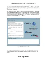
Страница 26: ... consists of a TCL based graphical user interface GUI with various input methods to initiate tests and report results The BTS GUI for the S2MB2 development board consists of three main tabs and three message windows for reporting test results The first tab is the Introduction tab This tab includes basic information and instructions about the available tests see Figure 5 Figure 5 BTS GUI Introducti...

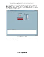
Страница 27: ...ing button is pushed The GUI s dipswitch and pushbuttons then display the boards User I O features The board s seven segment display and LEDs reflect the value selected on the slider and the checkbox values Figure 6 BTS GUI User IO Tab The third tab contains the tests for the Nios features These tests cover the SRAM Flash and Ethernet interfaces see Figure 7 ...

Страница 28: ...P server the test fails However the Ethernet chip is detected and the status of the DHCP acquisition is reported in the BTS Msgs window 3 3 2 DDR2 SDRAM DIMM Test This section describes the DDR2 SDRAM dual in line memory module DIMM test Refer to DDR2 SDRAM DIMM in section 3 1 6 for information on how to perform the test The DDR2 SDRAM DIMM test uses the Altera DDR2 SDRAM MegaCore function the exa...

Страница 29: ... for information on how to perform the test The DDR2 SDRAM test uses the Altera DDR2 SDRAM MegaCore function the example driver provided with the MegaCore function and some logic to indicate the status of the test This test reads and writes pseudo random binary sequence PRBS data to and from the DDR2 SDRAM The MegaCore function also includes a testbench and simulation instructions The DDR2 SDRAM t...

Страница 30: ...luded in the QDRII MegaCore function and four DDR2 SDRAM devices to test the DDR2 SDRAM interface The example driver is a self test module that issues read and write commands to the controller and checks the read data to produce the pass fail and test complete signals The example driver generates a pseudo random binary sequence PRBS that is written to the DDR2 SDRAM devices then read back and comp...

Страница 31: ...e EPM1270F256 device There are 104 of 120 I Os used in the design The controller utilizes the fast passive parallel FPP configuration mode of the Stratix II device family to quickly configure the device with the configuration data stored in the Flash memory device LEDS 7 0 AM29LV128MH FSE_D 7 0 User Design 0 FSE_D 7 0 Factory Design User Space FSE_A 26 0 MPGM 2 0 nSTATUS nCONFIG INIT_DONE CONF_DON...

Страница 32: ...e and even a website in the User Code Space Alternatively the Flash can be loaded with up to 6 user or demo designs and a large amount of software and a website in the User Code Space It is assumed that the Safe design would support Flash programming and web server support for potential documentation for the board and or the target FPGA or demo designs Stratix 2S60 16MB Flash Memory Map Block Name...

Страница 33: ... the page pointed to by MPGM 2 0 or SPGM 2 0 based on MSEL2 remote configuration enable SAFE design will be loaded if the User Design fails to load USER LEDs are driven through the MAX MAX II from the Stratix II LOADING LED blinks during a configuration attempt CONF_DONEn LED lights when the Factory Default image was loaded USER LED lights when a User Design was loaded from any page ERROR LED ligh...

Отзывы: