


Stratix II Memory Board 2 Rev A User Guide Rev 0.1
Altera Confidential
31
4
MAX/MAX II Configuration Controller
This section provides an explanation of the code that is used to program the
EPM1270F256 device which is used, in conjunction with the NIOS uP interface,
to configure the Stratix II device. This design is based on the Common
Configuration Specification’s “A-spec” that outlines a general CPLD-based Flash
configuration controller for Stratix II Boards.
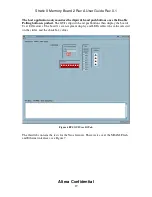
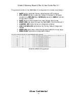
Figure 8
shows the block diagram of the MAX/MAX II configuration circuitry of the
Stratix II Memory Board 2. The design uses 129 of 256 macrocells in the
EPM1270F256 device. There are 104 of 120 I/Os used in the design. The
controller utilizes the fast passive parallel (FPP) configuration mode of the Stratix
II device family to quickly configure the device with the configuration data stored
in the Flash memory device.
LEDS(7:0)
AM29LV128MH
FSE_D(7:0)
User
Design 0
FSE_D(7:0)
Factory
Design
User Space
FSE_A(26:0)
M
P
G
M
(2
:0
)
nSTATUS
nCONFIG
INIT_DONE
CONF_DONE
R
E
S
E
Tn
FLASH_WEn
FLASH_RDY_BSYn
FLASH_CEn
FLASH_OEn
DCLK
User
Design 5
SPGM(2:0)
3.3V
PB
7256AE
TQ144
-or-
EPM1270
BGA256
PB
S
A
FE
n
CPLD_USER(1:0)
MAX_LED(7:0)
M
S
E
L(
3:
0)
R
U
_N
_L
U
3.3V
CONF_DONEn
FLASH_CEn
8 USER LEDS
USERn
LOADINGn
SAFEn
ERRORn
0
1
2
3
4
5
6
7
8
RESET
SAFE
CONFIG_D(7:0)
5
FLASH_BYTEn
FLASH_RSTn
MSEL(3:0)
8
STRATIX II .
FPGA .
Config
Block
Flash
Write
Design
Figure 8 MAX/MAX II Configuration Block Diagram


