background image

Publication No. HRMCP9 Rev. B 


Function Blocks  63 

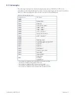
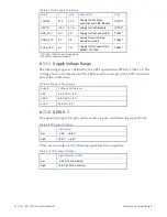
Table 7-7 BIOS Power-up Status 

Status 

LED color 

Power-up, still Reset state 

Red on (also the blue LED is on) 

BIOS early init 

Blink red 1Hz 

BIOS start POST 

Blink amber 1Hz 

BBIOS POSTA init 

Blink green 1Hz up to 4Hz 

OS boot 

Green on 

System halted or reset 

Red on 

The blue LED is the Hot Swap LED and is working according the Hot Swap 

specification. 

7.17.15  


Reset Button 

There is a Reset Button onboard. An external Reset button may be connected 
between the appropriate IO connector at the back side and GND. The PRST# on 

J7002_C17 (PICMG2.0) is used as Reset input only for the system board and is in this 

case, compatible to the onboard button. 


If the CR9 works as a System board: 
The push button will issue a hard power-on reset. The reset signal is active for all 

subsystems of the CR9. 


If the CR9 works as a Peripheral board: 
1) The push button will issue a hard power on reset. The reset signal is active for 

the CR9 including PMC modules, but will not reset other peripherals or the 
System board. 

2) The CR9 will signal a Hot Swap Insertion event when reset. 

7.17.16  


Speaker 

An internal speaker is implemented on the CR9 except on a CR9 N-Style (or 8-style). 
An external standard PC compatible speaker may be connected between the 

appropriate IO connector at the backside and +5 V. 


Содержание CR9 Series

Страница 1: ...Hardware Reference Manual CP9 CR9 CT9 Celeron M Pentium M 6U CompactPCI SBC with Hot Swap Publication No HRMCP9 Rev B ...

Страница 2: ...uipment WEEE Returns Abaco Systems is registered with an approved Producer Compliance Scheme PCS and subject to suitable contractual arrangements being in place will ensure WEEE is processed in accordance with the requirements of the WEEE Directive Abaco Systems will evaluate requests to take back products purchased by our customers before August 13 2005 on a case by case basis A WEEE management f...

Страница 3: ...ubscript and binary numbers have a b subscript The prefix 0x shows a hexadecimal number following the C programming language convention Thus One dozen 12D 0x0C 1100b The multipliers k M and G have their conventional scientific and engineering meanings of x103 x106 and x109 respectively and can be used to define a transfer rate The only exception to this is in the description of the size of memory ...

Страница 4: ...ww abaco com products cr9 https www abaco com search gss CT9 The following is a list of reference documentation related to CP9 CR9 CT9 CP9 Datasheet CR9 Datasheet CT9 Datasheet CR9 CT9 CP9 VR9 VP9 User s Manual for AMIBIOS8 Setup CR9 CT9 CP9 VR9 VP9 Board Specific Hardware Programmer s Manual AMIBIOS8 Check Point and Beep Code List AMIBIOS8 Error Messages Intelligent Platform Management Interface ...

Страница 5: ...ted and about the specific environment under which Abaco has tested these components Altitude Altitude air pressure and ambient temperature influence the thermal operation of the components described in this manual They have been developed and tested at about 500 m 1650 ft above sea level at a typical ambient temperature of 20 C 68 F Because of only marginal variations within a limited range of al...

Страница 6: ...ry in the Technical Support database and allocate it a unique Case number for use in any future correspondence Alternatively you may also contact Abaco s Technical Support via LINK support abaco com Returns If you need to return a product there is a Return Materials Authorization RMA form available via the website Embedded Support page LINK https www abaco com embedded support Do not return produc...

Страница 7: ... 2 Keyboard and Mouse 26 3 2 3 Video Monitor 27 3 2 4 Advice on Batteries 27 3 3 Installation of a Plug in Board 27 3 4 Installation of a Plug on Module Mezzanine 27 3 5 Installation of the Rear Transition Module CTM12 28 3 6 Initial Power On Operation 29 3 6 1 Entering the BIOS SETUP 29 4 Getting Started 30 4 1 Power Supply 30 4 2 Status Indicator Postcode and Beeps 30 4 3 Booting 31 4 4 Setup 32...

Страница 8: ...54 7 7 Keyboard and Mouse Controller 55 7 8 EIDE Interface 55 7 9 USB Interface 55 7 10 Serial Interface 55 7 11 Parallel Interface 56 7 12 Floppy Controller 56 7 13 Graphics Controller 56 7 13 1 Software Installation 57 7 14 PMC Interface 57 7 15 IPMI CT9 57 7 15 1 IPMB 58 7 15 2 Private I2 C 58 7 15 3 Software Installation 58 7 16 Ethernet Interface 58 7 16 1 Software Installation 58 7 17 Additi...

Страница 9: ...8 11 3 Electrical Clearance 73 8 11 4 Isolation 73 8 12 Placement Plan Component Side CR9 V2 74 8 13 Placement Plan Solder Side CR9 V2 75 A Transition Module CTM12 76 A 1 CTM12 Interfaces 78 A 1 1 EIDE Connector P1800 78 A 1 2 Ethernet Interface 10 100 1000BASE T P5000 and P5500 79 A 1 3 Parallel Interface LPT1 P2002 80 A 1 4 Serial Interfaces COM1 P2200 and COM2 P2201 P2203 80 A 1 5 VGA Interface...

Страница 10: ...Figure 5 6 Keyboard and Mouse Connector Layout 41 Figure 5 7 Ethernet Connector Location 41 Figure 5 8 Ethernet Connector Layout 41 Figure 5 9 COM1 Location 42 Figure 5 10 VGA Connector Location 43 Figure 5 11 USB Connector Location 44 Figure 5 12 USB Connector Layout 44 Figure 8 1 Battery Current Versus Temperature 66 Figure 8 2 Battery Current Versus Time 67 Figure 8 3 Battery Removal 68 Figure ...

Страница 11: ...le 6 1 Memory Area Assignments 49 Table 6 2 Standard Register Set 50 Table 6 3 Interrupt Assignments 51 Table 7 1 Interval Timer Functions 54 Table 7 2 Parallel Interface Options 56 Table 7 3 IPMB Backplane Pin Assignments 58 Table 7 4 Supported Operating Systems 58 Table 7 5 SMBus Devices 60 Table 7 6 Power Management Events 61 Table 7 7 BIOS Power up Status 63 Table 8 1 Power Consumption CPU Dep...

Страница 12: ... Pin Assignments 82 Table A 9 USB Connector 10 pin header Pin Assignments 83 Table A 10 Floppy Connector Pin Assignments 83 Table A 11 Miscellaneous Connector Pin Assignments 84 Table A 12 PMC I O Onboard PIM Connector Pin Assignments 85 Table A 13 PMC I O 64 pin header Connector Pin Assignments 86 Table A 14 Power Connector Pin Assignments 87 Table A 15 Power IN OUT Connector Pin Assignments 87 T...

Страница 13: ...ing information are also provided A number of expansion and add on products are available for the CR9 CP9 and CT9 The CTM12 transition module and the PMC module are described in appendices to this manual Please observe all safety instructions when handling Abaco products as outlined in the unpacking and installation chapters This chapter describes features capabilities and compatibility of the CR9...

Страница 14: ...No HRMCP9 Rev B 1 1 Board Design The CR9 s minimized board size and the large number of interfaces and functions allow the CR9 to be used in many applications See the following block diagram for the board design Figure 1 1 Block Diagram of CR9 Board ...

Страница 15: ...e 420 Go series high performance graphics controller with integrated DDR memory 16 or 32 MByte max resolution at DVI port 1024x768 at CRT 1600x1200 Version 3 x RoHS version uses the ATI Mobility Radeon graphics controller with 128 256 bit 2D 3D and multimedia graphics accelerator 16 MByte to 64 MByte DDR memory max resolution 1600 x 1200 analog and 1024 x 768 DVI USB One front and 4 rear USB 2 0 p...

Страница 16: ...e at the rear connectors With PCB version V2 the 64 bit PMC lot is PCI X capable with 66 100 133 MHz CPCI System slot Up to 7 peripheral slots 64 Bit CPCI 33 MHz with Hint HB6 bridge Up to 4 peripheral slots 64 Bit 66 MHz Standard backplanes can be used Onboard Pull up resistors are optimized for 3 3 V I O voltage but 5 V I O can also be used for 33 MHz CPCI I O Slot CR9 works as peripheral board ...

Страница 17: ...FCC A H110 Backplanes The CT9 can be optionally ordered without connector J7004 CPCI J4 assembled for backplanes providing H110 functionality As a consequence some rear I O will not be available Please check in Chapter 5 Interfaces for more details Styles available Table 1 1 Styles Available CR9 non ROHS C D I H R N CR9 RoHS 1 2 3 4 6 8 Front panel x x x x x Extended temp x x x x Parts soldered x ...

Страница 18: ...subsystems which cannot provide a useful function on their own do not need certification Certification can only be granted to complete and operational systems There are authorized testing agencies regulatory organizations and laboratories who will issue certificates of compliance after system testing Abaco designs and tests all their products for EMI EMC conformance Where Abaco supplies a complete...

Страница 19: ...required in EU countries for equipment which is used or operated by the end user Products sold or transferred between companies or operated on company premises factory floor laboratory do not need CE certification CE certification can only be granted to complete and operational systems Boards or subsystems which cannot provide a useful function on their own do not need CE certification Abaco desig...

Страница 20: ...ins the following items Table 2 1 Delivery Volume Qty Item Purpose 1 CR9 or CP9 or CT9 CompactPCI Single Board Computer 1 CDROM Technical Product Information with driver software and manuals in Adobe Acrobat PDF format The manual files are also available through our website https www abaco com 2 2 Available Accessories The following table lists accessory options which are available for the CR9 Tab...

Страница 21: ...ther when static easily builds up Only after ensuring that both you and the surrounding area are protected from ESD carefully remove the board or module from the shipping carton by grasping it by the front panel and the connectors Place the board in its antistatic bag flat down on a suitable surface You may then remove the board from the antistatic bag by tearing the ESD warning labels 2 4 Warning...

Страница 22: ...sitive modules If the product contains batteries please do not place the board on conductive surfaces antistatic plastic or sponge which can cause shocks and lead to battery or board trace damage Please do not exceed the specified operational temperatures Note that batteries and storage devices might also have temperature restrictions Keep all original packaging material for future storage or warr...

Страница 23: ... the CR9 is critical to ensure proper operation and long term reliability When unpacking the board and whenever handling it thereafter be sure to hold the board by the front panel or the card ejectors as shown in the drawing on the left Do not hold the board by the circuit card edges the heat sink or the connectors ...

Страница 24: ...24 CP9 CR9 CT9 Celeron M Pentium M Publication No HRMCP9 Rev B Figure 2 2 Handling the CR9 Board ...

Страница 25: ...perly restore the power 3 1 1 General Advisories Before installing or removing any board please ensure that the system power and external supplies have been turned off Check that jumpers and mezzanines are correctly configured for your application Mount the board mezzanine or transition module very carefully See also sections on additional advisories below Do not restore power until you are sure t...

Страница 26: ...al CPU board in the system slot for providing system clock arbiter function and more Please make sure that you do not have the power supply turned ON when the CR9 is plugged into your backplane 3 2 2 Keyboard and Mouse You should have a compatible keyboard for initial system operation Depending on your application this keyboard may be a standard full travel keyboard or one which utilizes membrane ...

Страница 27: ...of a Plug in Board Boards are installed in a CPCI or VMEbus chassis by carefully sliding them into the guide rails inserting them all the way until the handles can be operated to seat and lock the board in place Handles typically have a lock snap lever to unlock them when extracting a board Older boards may have screws instead of handles to secure the board in place Figure 3 1 6U Board Insertion i...

Страница 28: ...dule you either can connect a DVI panel or a standard VGA Monitor but not both at the same time Plug your video monitor into this connector Make sure that your selected chassis supports this type of rear I O transition module After making sure that you have installed the CR9 properly into your CPCI backplane apply power to your video monitor and then the CPCI supply When the board is completely re...

Страница 29: ...ay also press the DELETE key when the LED goes from blinking orange to blinking green Consult the AMI BIOS for CR9 CP9 CT9 User s and Programmer s Manual for further information on how to change settings and configurations If the board does not perform as described above some damage may have occurred in shipping or the board is not installed or setup properly Contact Abaco technical support as des...

Страница 30: ...rear contacts of the bus connectors or unused power connectors to measure because measuring the voltages at the used power connectors can result in wrong values which are caused by the high current flowing The 12 V are less critical but 5 V and 3 3 V should reach their nominal value when measuring with a multimeter If the voltages are less than 5 0 V or 3 3 V then short voltage drops while the CPU...

Страница 31: ...alue The continuous red Status LED shows that all circuitry is in reset All onboard DC DC converters are ramped up If all onboard supply voltages are at their correct values the power good status is acknowledged to all onboard devices and the red LED is switched off On the CR9 family the blue Hot Swap LED is switched off when the onboard PCI reset is released Especially when the battery is removed...

Страница 32: ...ou have to press the keyboard DEL key at the right moment Especially when using a slow starting monitor it might be too late to wait for the CRT to show the message Press DEL to enter Setup Better look for the LED and press DEL as soon as the LED goes from orange to green blinking When you are using add on cards with external BIOS you can hit the DEL key while their BIOS runs i e SCSI BIOS device ...

Страница 33: ...aco has no drivers to support these functionalities The handling of the blue LED is also done within the necessary drivers Do not expect the blue LED to go on and off according to the CPCI specification if no driver is loaded 4 6 Unexpected Results Whenever the CR9 unexpectedly issues a reset and starts booting again you may want to know the reset source For this reason a set of special registers ...

Страница 34: ... and a pin assignment table as well as notes on certain signal line characteristics if necessary For interfaces of the transition module please refer to the appropriate chapters found in Appendix Transition Module CTM12 Figure 5 1 Location of Components on Board and Front Panel 5 1 Front Panel Interfaces Refer to the next drawing for the location of interfaces on the front panel of the CR9 and CT9...

Страница 35: ...I Connector Reference The CPCI specification numbers the CPCI connectors from bottom to top J1 J2 J3 J4 and J5 The CPCI connectors on the CR9 are J7001 J7002 J7003 J7004 and J7005 respectively Table 5 1 Signal Name Groups Signal groups Determiner floppy disk controller signals FD hard disk controller signals HD and HD Parallel port L1 and L1 COM1 COM2 signals C1 C2 VGA signals VGA Universal Serial...

Страница 36: ...10 AD49 AD48 AD47 GND AD46 GND 9 AD52 GND VIO b AD51 AD50 GND 8 AD56 AD55 AD54 GND AD53 GND 7 AD59 GND VIO b AD58 AD57 GND 6 AD63 AD62 AD61 GND AD60 GND 5 C BE5 64EN VIO b C BE4 PAR64 GND 4 VIO b NC C BE7 GND C BE6 GND 3 CLK4 GND GNT3 REQ4 GNT4 GND 2 CLK2 CLK3 SYSEN GNT2 REQ3 GND 1 CLK1 GND REQ1 GNT1 REQ2 GND J7001 A B C D E F 25 5V REQ64 ENUM 3 3V 5V GND 24 AD01 5V LVIO a b AD00 ACK64 GND 23 3 3V...

Страница 37: ...Connectors J7003 J7004 and J7005 J7003 A B C D E F 19 GND GND GND GND GND GND 18 LPA_DA LPA_DA GND LPA_DC LPA_DC GND 17 LPA_DB LPA_DB GND LPA_DD LPA_DD GND 16 LPB_DA LPB_DA GND LPB_DC LPB_DC GND 15 LPB_DB LPB_DB GND LPB_DD LPB_DD GND 14 VCC3 a VCC3 a VCC3 a VCC a VCC a GND 13 PMC1IO_05 PMC1IO_04 PMC1IO_03 PMC1IO_02 PMC1IO_01 GND 12 PMC1IO_10 PMC1IO_09 PMC1IO_08 PMC1IO_07 PMC1IO_06 GND 11 PMC1IO_15...

Страница 38: ...TRKO L_STRO MS_CLK VGA_VSYNC GND 17 L_ERROR FD_RDAT L_AFED MS_DATA VGA_DDCD GND 16 L_PE L_SLIN L_INIT KB_CLK VGA_DDCC GND 15 L_SLCT L_BUSY L_ACK KB_DATA HOTPLG GND 12 14 KEY KEY KEY KEY KEY KEY 11 VCCOFF NC VBATIN SPEAKER GPIO1 GND 10 NC NC NC RST_BUT GPIO0 GND 9 NC NC NC GPIO2 GPIO3 GND 8 NC NC NC GPIO4 GPIO5 GND 7 NC NC NC GPIO6 GPIO7 GND 6 NC NC NC GND GND GND 5 M1LINK1000 M2LINK1000 NC TX1 TXC...

Страница 39: ...C2IO_52 PMC2IO_51 GND 11 PMC2IO_60 PMC2IO_59 PMC2IO_58 PMC2IO_57 PMC2IO_56 GND 10 PMC2VIO PMC2IO_64 PMC2IO_63 PMC2IO_62 PMC2IO_61 GND 9 C1_DCD TXD C1_DSR TXD PHD_CS0 PHD_IOR PHD_IOW GND 8 C1_RXD RTS C1_RTS RTS PHD_A0 PHD_D08 PHD_D07 GND 7 C1_TXD CTS C1_CTS CTS PHD_IRQ PHD_D09 PHD_D06 GND 6 C1_DTR RXD C1_RI RXD PHD_RDY PHD_D10 PHD_D05 GND 5 C2_DCD TXD C2_DSR TXD PHD_DAK PHD_D11 PHD_D04 GND 4 C2_RXD...

Страница 40: ... 20 19 GND GND 22 21 HD_DRQ0 GND 24 23 HD_IOW GND 26 25 HD_IOR NC 28 27 HD_RDY GND 30 29 HD_DAK NC 32 31 HD_IRQ DIAG 34 33 HD_A1 HD_A2 36 35 HD_A0 HD_CS1 38 37 HD_CS0 GND 40 39 DASP 5V 42 41 5V NC 44 43 GND 5 2 5 Keyboard and PS 2 Mouse Interface P2001 The CR9 allows an easy adaptation of a keyboard to a standard 6 pin MINIDIN connector Also a PS 2 mouse can be connected directly or via an externa...

Страница 41: ... a the Fused 5 V pin is fused with a 2 A fuse For normal operation don t exceed 100 mA current The used fuse does automatically recover if the over current is resolved 5 2 6 Ethernet Interface U5600 and U5650 The Ethernet output front or rear can be selected via order When ordered with front option the connectors are located in the front panel Figure 5 7 Ethernet Connector Location Figure 5 8 Ethe...

Страница 42: ...e rear I O is compliant with the PICMG 2 16 Switched Packet Backplane specification The Ethernet interface can also be accessed via the CTM12 transition module see Ethernet Interface 10 100 1000BASE T P5000 and P5500 for connector type and pin assignment 5 2 7 Serial Port COM1 P2201 The CR9 offers two RS232 serial ports All COM ports are accessible via the transition module and additionally COM1 i...

Страница 43: ...gnals are available at the front panel on a standard 15 pin female D Sub connector Figure 5 10 VGA Connector Location Table 5 9 VGA Connector Pin Assignments Name P4200 RED 1 GREEN 2 BLUE 3 HSYNC 13 VSYNC 14 DDC Data 12 DDC Clock 15 Fused 5 V a 9 GND 5 6 7 8 10 NC 4 11 a the Fused 5 V pin is fused with a 2 A fuse For normal operation don t exceed 100 mA current The used fuse does automatically rec...

Страница 44: ...s of the onboard PMC1 connector The PMC1 slot is 64 bit and 66 MHz capable and works with the internal second PCI bus of the P64H2 PCI Bridge If an installed PMC card operates at 33 MHz only the PCI bus speed is reduced to 33 MHz With board revision V2 and higher this slot is PCI X capable with 66 100 133 MHz The PMC is electrical and mechanical compliant to the specification IEEE 1386 and 1386 1 ...

Страница 45: ...D19 AD18 AD51 29 30 5 V GND AD50 V I O AD16 AD49 31 32 AD17 C BE2 GND FRAME GND GND 33 34 GND AD30 IDSELB AD48 GND TRDY AD47 35 36 IRDY 3 3V AD46 DEVSEL GND AD45 37 38 5 V STOP GND PCIXCAP PERR V I O 39 40 LOCK GND AD44 Reserved 3 3 V AD43 41 42 RES SERR AD42 PAR C BE1 AD41 43 44 GND GND GND V I O AD14 GND 45 46 AD15 AD13 AD40 AD12 M66EN AD39 47 48 AD11 AD10 AD38 AD9 AD8 AD37 49 50 5V 3 3 V GND GN...

Страница 46: ...with the internal primary PCI bus of the I O Controller Hub The PMC is electrical and mechanical compliant to the specification IEEE 1386 and 1386 1 with enhancements of the Processor PMC Standard VITA 32 2003 Check for possible height incompatibility in Features and Specifications sections of this manual The enhancements provide pins for a second device IDSELB and REQB GNTB but don t support a mo...

Страница 47: ...7 28 AD21 AD20 AD19 AD18 29 30 5 V GND V I O AD16 31 32 AD17 C BE2 FRAME GND 33 34 GND AD29 IDSELB GND TRDY 35 36 IRDY 3 3 V DEVSEL GND 37 38 5 V STOP GND PERR 39 40 LOCK GND Reserved 3 3 V 41 42 RES SERR PAR C BE1 43 44 GND GND V I O AD14 45 46 AD15 AD13 AD12 GND 47 48 AD11 AD10 AD9 AD8 49 50 5 V 3 3 V GND AD7 51 52 C BE0 REQB AD6 3 3 V 53 54 AD5 GNTB AD4 Reserved 55 56 GND GND V I O NC 57 58 AD3...

Страница 48: ...d so on The x denotes PMC1 or PMC2 respectively All traces are not connected to any signal onboard and no pairs or length adjusted traces are used to route this signals to the backplane connectors 5 3 Transition Module Please refer to the appendix chapters for interface location and connector pin assignments for the optional extension boards and transition modules ...

Страница 49: ... Ethernet E0000 FFFFF 128 KByte System BIOS 100000 3FFFFFFF Depends on avail DRAM Extended RAM 4000000 FFFBFFFF Depends on avail DRAM Dynamically used by PCI devices FFF80000 FFFFFFFF 512 KByte System BIOS 6 2 Register Set The following section provides an overview of the registers located in the I O address area of the CR9 NOTE The address location of PCI devices such as SCSI or Ethernet are not ...

Страница 50: ...e register 00A0 00A1 Interrupt Controller 2 00B2 00B3 Power Management 00C0 00DE DMA Controller 2 00F0 00F1 Coprocessor 0160 016F Reserved b 0170 0177 Secondary EIDE 01F0 01F7 Primary EIDE 0278 027F LPT a 02E8 02EF COM port a 02F8 02FF COM port a 0378 037F LPT a 03BC 03BF LPT a 03E8 03EF COM port a 03F2 03F7 Floppy 03F8 03FF COM1 port a a Via setup three address ranges can be defined for the paral...

Страница 51: ...IRQ05 LPT1 a PnP PCI b IRQ06 Floppy Disk Controller IRQ07 LPT1 a PnP PCI b INTC2 IRQ08 Real Time Clock IRQ09 Power Management Contr PCI b IRQ10 PnP PCI b IRQ11 PnP PCI b IRQ12 PS 2 Mouse c IRQ13 Numeric Coprocessor IRQ14 Rear EIDE d IRQ15 Onboard EIDE e NMI Parity Error ECC Error System Error a This interrupt is available when no Interrupt Service Routine is installed b Interrupts are available fo...

Страница 52: ...s are Method of Interrupt Transmission The I O APIC transmits interrupts through a three wire bus and interrupts are handled without need for the processor to run an interrupt acknowledge cycle Interrupt Priority The priority of interrupts in the I O APIC is independent of the interrupt number For example interrupt 10 may be given a higher priority than interrupt 3 More Interrupts The I O APIC in ...

Страница 53: ...f on cycle only 7 2 Memory Controller The memory controller in the CR9 supports double data rate synchronous DRAM DDR SDRAM with a data bus width of 64 bits ECC One two or four banks are provided by the CR9 with a size of either 256 MByte or 512 MByte This results in a minimum memory size of 256 MByte and a maximum size of 2 GByte 7 3 DMA Controller In standard AT compatible PCs as well as on the ...

Страница 54: ...gives an overview over the 8254 functions Table 7 1 Interval Timer Functions Interval Timer Functions Function Counter 0 System Timer Gate Always on Clock In 1 193 MHz OSC 12 Out IRQ0 INT1 Function Counter 1 Refresh Request Gate Always on Clock In 1 193 MHz OSC 12 Out Refresh Request Function Counter 2 Speaker Tone Gate Programmable via Port 061 Clock In 1 193 MHz OSC 12 Out Speaker The counter ti...

Страница 55: ...our drive The optional 2 5 onboard disk is connected to an onboard EIDE connector secondary EIDE interface Using EIDE and SCSI devices MS DOS 6 22 can handle up to seven hard disks The PC allows the simultaneous use of EIDE and SCSI hard disks BIOS setup allows reordering drives to boot from either SCSI or EIDE drives NOTE For correct operation of the EIDE interface a maximum cable length of 12 in...

Страница 56: ...nd can occupy three address ranges The address range 3BC cannot be used with EPP operation 7 12 Floppy Controller The CR9 floppy controller is fully compatible with the PC8477 containing a superset of the NEC uPD72065B and the N82077AA The floppy controller uses various I O addresses in the PC I O address space 7 13 Graphics Controller The Graphic Controller NVIDIA GeForce 4 420 Go used in version...

Страница 57: ... drivers The Technical Product Information CD ROM supplied with the CR9 includes the most commonly used software drivers and utilities 7 14 PMC Interface The PCI Mezzanine Card PMC Interface is an additional slot for parallel mounted expander or option cards Please see Appendix PCI Mezzanine Card PMC on page 89 of this manual for further details The CR9 PMC Connector interface is described on page...

Страница 58: ...ed software drivers and utilities 7 16 Ethernet Interface The Ethernet controller 82546GB from Intel used with the CR9 is a high performance dual Gigabit Ethernet 10 100 1000 Mbit PCI controller Both channels are available on the CR9 Front or rear Ethernet can be selected via order For registration and identification of a workstation in a LAN a unique ID number is required Each network card is ass...

Страница 59: ...t Insertion by which CR9 is installed in a live system as a non system CPU Hot Extraction which means the CR9 is removed from a live system as a non system CPU Hardware Connection Process Power Up Down of the CR9 onboard voltages Software Connection Process Connection disconnection of the software layer s At the end of the Physical Connection Process the shortest Pin has connection the Hot Swap co...

Страница 60: ... handled by BIOS It is strongly recommended not to access these devices by user software An X at bit 0 represents the R W bit 7 17 3 SMBus External IPMB The Intelligent Platform Management Bus IPMB is available on the J7002 CPCI connector for external use External access via IPMB to the onboard SMBus devices can only be done via the IPMI controller For more information please see the IPMB descript...

Страница 61: ...vents Table 7 6 Power Management Events Event Description ENUM Wake CR9 a if a non system board is removed or inserted REMOVE Wake CR9 if user wants to remove this CR9 Wake on LAN Wake CR9 by Ethernet event Wake on IO Wake CR9 by IO device i e Modem KB MS etc a CR9 in System slot 7 17 8 INTP INTS The INTP and INTS signals PICMG2 0 are available on the J7001_D4 E4 For CR9 in System Slot the high ac...

Страница 62: ... GPIO 0 7 Eight GPIO pins are available on J7004 These pins can be used for I O functions with output 3 3 V signals as well as 5 V tolerant inputs For more information please see the Board Specific Hardware Programmer s Manual 7 17 12 Watchdog For security of application software the CR9 offers a software controlled hardware two stage watchdog with independent count values for each stage First sta...

Страница 63: ...RST on J7002_C17 PICMG2 0 is used as Reset input only for the system board and is in this case compatible to the onboard button If the CR9 works as a System board The push button will issue a hard power on reset The reset signal is active for all subsystems of the CR9 If the CR9 works as a Peripheral board 1 The push button will issue a hard power on reset The reset signal is active for the CR9 in...

Страница 64: ...specification allows This is to be checked when planning to insert a PMC mezzanine module in the center of a 6U board PMC1 If no PMC is inserted into this mezzanine slot then there is no mechanical height violation 8 5 Weight Approx 650 g with front panel HDD and heat sink Depending on model and style 8 6 RoHS Compliance Version 2 of CR9 is only available in Non RoHS Version 3 of CR9 is available ...

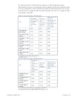
Страница 65: ... 0 7 A 0 9 A 0 9 A Celeron M 1 0 GHz 90 nm 0 7 A 0 9 A 0 9 A Pentium M 1 1 GHz 130 nm 1 2 A 1 6 A 2 3 A Pentium M 1 4 GHz 90 nm 1 2 A 1 6 A 2 3 A Pentium M 1 6 GHz 130 nm 2 7 A 3 5 A 5 4 A Pentium M 1 8 GHz 90 nm 2 5 A 3 0 A 4 5 A Celeron M 1 3 GHz 130 nm 2 2 A 2 6 A 4 6 A for every 25 C more please add around 10 estimated values Table 8 2 Power Consumption DRAM Dependent CR9 DOS prompt or CPU run...

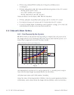
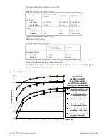
Страница 66: ...wn from this source may not exceed 1 0 A 8 8 Onboard Lithium Battery 8 8 1 Not Powered by the System BR1225 50 mAh estimated life time depending on temperature and power status The diagram below shows discharge if board is not powered from the system i e if battery has to supply all current for the clock circuits Figure 8 1 Battery Current Versus Temperature At temperatures lower than 25 C use the...

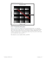
Страница 67: ...self discharge happens Typical self discharge rates are less than 0 3 percent per year with respect to a fully loaded battery at an ambient temperature of 25 C Self discharge rates increase by less than 3 percent per year for temperature values up to 95 C The battery has a user accessible holder on the CR9 Discharge Battery BR1225 0 01 0 10 1 00 10 00 100 00 0 1 1 10 100 Discharge Current µA Disch...

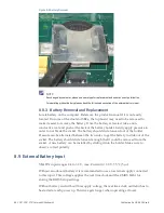
Страница 68: ... Gently apply pressure in order to not break the socket The battery should slide forward out of the holder Pressure can be alternated between the two sides to get the battery to slide out of the socket The battery should slide forward enough that it could be removed from the socket A new battery can be installed by sliding it into the holder Make sure to observe correct polarity 8 9 External Batte...

Страница 69: ... products from Abaco It is still recommended to use an external supply voltage to this battery input to avoid the power on oscillator start time and to keep the date and time information 8 10 Environment Conditions Ambient temperatures and humidity values for the CR9 Table 8 3 Environment Conditions C D 1 2 Style I H R N 3 4 6 8 Style High Temperature Storage see note below Operating see diagram b...

Страница 70: ... capable to be used in a vacuum environment All other styles contain either batteries and do not have the possibility to be cooled without airflow For highest operating temperatures C D I H R 1 2 3 4 6 Style please refer to the following diagram Figure 8 4 Temperature vs Airspeed CR9 CT9 CP9 no PMC no HDD next slot occupied worst thermal contact running full cache access 30 0 40 0 50 0 60 0 70 0 8...

Страница 71: ...be taken into consideration Both limits are valid with the low power CPUs running at 600 MHz or 1100 MHz For higher CPU frequencies the maximum operating temperature is limited by the CPU already When using an onboard hard disk drive not with flash disk the operating temperature is limited to 50 C When using one or two PMC modules please consider their power consumption and thermal limits in calcu...

Страница 72: ...exas Instruments 8 11 1 Supply Voltage Range The following ranges are defined by the CPCI specification PICMG 2 0 Rev 3 0 The voltages have to be measured at the CR9 board for example at the CPCI connector pins at the solder side Table 8 8 Supply Voltage Range Supply Voltage and tolerance 5 V 5 0 V 5 3 3 3 V 3 3 V 5 3 12 V 12 0 V 5 8 11 2 GPIO 0 7 This general purpose I O pins can be used as input...

Страница 73: ...rs uncoated sea level to 3050 m These rules are in accordance with IPC 2221 requirements 8 11 4 Isolation The Isolation of the Ethernet outputs whether front or rear is limited to 500 V peak against GND and any other supply voltage By itself the onboard digital ground GND and the front panel chassis frame ground FGND are isolated on the CR9 with a layout distance of more than 0 3 mm in all PCB lay...

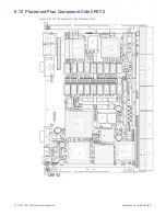
Страница 74: ...74 CP9 CR9 CT9 Celeron M Pentium M Publication No HRMCP9 Rev B 8 12 Placement Plan Component Side CR9 V2 Figure 8 5 CR9 V2 Component Side Placement Plan ...

Страница 75: ...Publication No HRMCP9 Rev B Specifications 75 8 13 Placement Plan Solder Side CR9 V2 Figure 8 6 CR9 V2 Solder Side Placement Plan ...

Страница 76: ... the backplane Without the need for Hot Swap the external drives may be connected direct to the power supply and P7700 and P7701 need not to be connected except the 12 V from P7700 for the PIM connectors P7100 P7200 are needed NOTE You either can use a DVI display on P4100 or a standard VGA Monitor Display connected to P4001 or a standard VGA Monitor Display via a DVI to VGA adaptor connected to P...

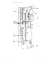
Страница 77: ...Publication No HRMCP9 Rev B Transition Module CTM12 77 Figure A 1 CTM12 Component Locations ...

Страница 78: ...d drives The cable length must not exceed 30 cm It is recommended to use an 80 pin high density cable for UDMA 3 and higher transfer Table A 1 CTM12 EIDE Connector Name P1800 Name GND 2 1 RST_DRV HD_D8 4 3 HD_D7 HD_D9 6 5 HD_D6 HD_D10 8 7 HD_D5 HD_D11 10 9 HD_D4 HD_D12 12 11 HD_D3 HD_D13 14 13 HD_D2 HD_D14 16 15 HD_D1 HD_D15 18 17 HD_D0 NC 20 19 GND GND 22 21 HD_DRQ0 GND 24 23 HD_IOW GND 26 25 HD_...

Страница 79: ...ernet Connector Pin Assignments Name 10 100BASE TX Name 1000BASE T Ethernet1 2 TxD LP_DA 1 TxD LP_DA 2 RxD LP_DB 3 NC LP_DC 4 NC LP_DC 5 RxD LP_DB 6 NC LP_DD 7 NC LP_DD 8 Two LEDs LED1 and LED2 are integrated in each of the RJ45 connector These LEDs indicates the link status of the interface Table A 3 CTM12 Ethernet Connector LED LED1 green Function green General link blink green orange General li...

Страница 80: ...M12 for normal operation don t exceed 100 mA at this pin A 1 4 Serial Interfaces COM1 P2200 and COM2 P2201 P2203 The CR9 offers two RS232 serial ports All COM ports are accessible via the Transition module at 10 pin headers and are software selectable for RS232 or RS422 485 operation The RS485 output drivers can be enabled or disabled with the DTR signal An active DTR means the drivers to be enabl...

Страница 81: ...on P4100 or a standard VGA Monitor Display connected to P4001 or a standard VGA Monitor Display via a DVI to VGA adaptor connected to P4100 You never can use two display devices connected to the transition module If you want to have two display outputs you will have to connect one to the front of the CR9 and one to the rear transition module Table A 6 VGA Connector Pin Assignments Name P4001 RED 2...

Страница 82: ...2 GND 11 GND 23 TXC TMDS Clock 12 NC 24 TXC TMDS Clock Table A 8 DVI Connector Analog Pin Assignments Pin Signal name C1 RED Analog Red Video C2 GREEN Analog Green Video C3 BLUE Analog Blue Video C4 HSYNC Analog Horizontal Sync C5 GND a 5 V supplied by the CR9 and fused with max 2 A at CTM12 for normal operation don t exceed 100 mA at this pin A 1 7 USB Connector P2005 Four channels are available ...

Страница 83: ...floppy drive please use a non twisted 34 pin flat cable connected to P2004 Alternatively you can use a 26 pin foil cable connector P2003 Table A 10 Floppy Connector Pin Assignments Name P2003 P2004 INDEX 2 8 DRVSEL 4 12 DSKCHG 6 34 MOTOR 10 16 DIR 12 18 STEP 14 20 WRDATA 16 22 WGATE 18 24 TRACK0 20 26 WRPROT 22 28 RDDATA 24 30 HDSEL 26 32 GND 15 17 19 21 23 25 1 3 5 7 9 11 13 15 17 19 21 23 25 27 ...

Страница 84: ... at CTM12 for normal operation don t exceed 100 mA at this pin b VBATIN is used to connect an external battery to CR9 For description please check the section External Battery Input c VIO is the I O voltage of the PMC slot and is connected to 5 V on the CT A 1 10 PMC I O Connectors The PMC I O signals of both PMC slots are either available at 64 pin male headers P7101 P7201 or via VITA36 compliant...

Страница 85: ..._33 33 34 GND PMCxIO_34 PMCxIO_35 35 36 PMCxIO_36 5 V a PMCxIO_37 37 38 PMCxIO_38 PMCxIO_39 39 40 PMCxIO_40 PMCxIO_41 41 42 3 3 V a PMCxIO_42 PMCxIO_43 43 44 PMCxIO_44 GND PMCxIO_45 45 46 PMCxIO_46 PMCxIO_47 47 48 PMCxIO_48 PMCxIO_49 49 50 GND PMCxIO_50 PMCxIO_51 51 52 PMCxIO_52 5 V a PMCxIO_53 53 54 PMCxIO_54 PMCxIO_55 55 56 PMCxIO_56 PMCxIO_57 57 58 3 3 V a PMCxIO_58 PMCxIO_59 59 60 PMCxIO_60 12...

Страница 86: ...19 20 PMCxIO_20 PMCxIO_21 21 22 PMCxIO_22 PMCxIO_23 23 24 PMCxIO_24 PMCxIO_25 25 26 PMCxIO_26 PMCxIO_27 27 28 PMCxIO_28 PMCxIO_29 29 30 PMCxIO_30 PMCxIO_31 31 32 PMCxIO_32 PMCxIO_33 33 34 PMCxIO_34 PMCxIO_35 35 36 PMCxIO_36 PMCxIO_37 37 38 PMCxIO_38 PMCxIO_39 39 40 PMCxIO_40 PMCxIO_41 41 42 PMCxIO_42 PMCxIO_43 43 44 PMCxIO_44 PMCxIO_45 45 46 PMCxIO_46 PMCxIO_47 47 48 PMCxIO_48 PMCxIO_49 49 50 PMCx...

Страница 87: ... P7701 In case of Hot Swap insertion or extraction phase of the CR9 the CTM12 provides the possibility of switch off the power to external storage devices The voltage 5 V and 12 V between power in P7700 and power out P7701 controls a Hot Swap controller via MOSFETs The Hot Swap controller cut the voltage when the signal VCCOFF is low VCCOFF is controlled by the Hot Swap at the CR9 In case of over ...

Страница 88: ...88 CP9 CR9 CT9 Celeron M Pentium M Publication No HRMCP9 Rev B A 2 Placement Plan Figure A 4 Placement Plan CTM12 ...

Страница 89: ... compatible PMC Cards B 1 Electrical Characteristics Table B 1 Electrical Characteristics Parameter Comment Value I3 3V Max current on 3 3 V Pins 2 1 A c I5V Max current on 5 V Pins 1 2 A c I 12V Max current on 12 V Pin 0 1 A I 12V a Max current on 12 V Pin 0 1 A V I O b Voltage for PCI IO 3 3 V or 5 V P Max power consumption total 7 5 W a 12 V must be connected to the backplane b The appropriate ...

Страница 90: ...90 CP9 CR9 CT9 Celeron M Pentium M Publication No HRMCP9 Rev B Figure B 1 Mount PMC Board to CR9 ...

Страница 91: ... ITS CONTENTS ARE PROVIDED AS IS WITH NO REPRESENTATIONS OR WARRANTIES OF ANY KIND WHETHER EXPRESS OR IMPLIED INCLUDING BUT NOT LIMITED TO WARRANTIES OF DESIGN MERCHANTABILITY OR FITNESS FOR A PARTICULAR PURPOSE ALL OTHER LIABILITY ARISING FROM RELIANCE ON ANY INFORMATION CONTAINED HEREIN IS EXPRESSLY DISCLAIMED Abaco Systems Information Centers Americas 1 866 652 2226 866 OK ABACO or 1 256 880 04...

Отзывы: