background image

AXI Bridge for PCI Express v2.4

www.xilinx.com

74

PG055 June 4, 2014

Chapter 4: 

Design Flow Steps

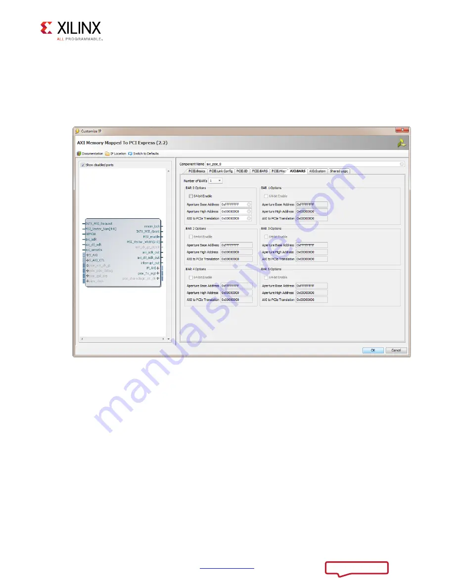
AXI Base Address Registers

The AXI Base Address Registers (BARs) screen shown in 

Figure 4-6

 sets the AXI base address 

registers and the translation between AXI Memory space and PCI Express Memory space. 

Each BAR has a Base Address, High Address, and translation field which can be configured 

through the Vivado IDE.

Number of BARs

Indicates the number of AXI BARs enabled.The BARs are enabled sequentially.

64-bit Enable

Indicates if the AXI Base Address Register is 64-bit addressable. Selecting a 64-bit BAR 

consumes the subsequent BAR.

Aperture Base Address

Sets the base address for the address range associated to the BAR. You should edit this 

parameter to fit design requirements.

X-Ref Target - Figure 4-6

Figure 4-6: 

AXI Base Address Registers

Send Feedback

Summary of Contents for LogiCORE IP AXI

Page 1: ...LogiCORE IP AXI Bridge for PCI Express v2 4 Product Guide Vivado Design Suite PG055 June 4 2014 ...

Page 2: ... Resource Utilization 11 Port Descriptions 12 Bridge Parameters 15 Parameter Dependencies 22 Memory Map 26 Chapter 3 Designing with the Core General Design Guidelines 42 Clocking 42 Resets 43 Shared Logic 44 AXI Transactions for PCIe 50 Transaction Ordering for PCIe 51 Address Translation 52 Interrupts 56 Malformed TLP 58 Abnormal Conditions 58 Root Port 62 Chapter 4 Design Flow Steps Customizing ...

Page 3: ...tput Structure 83 Chapter 6 Test Bench Appendix A Migrating and Upgrading Migrating to the Vivado Design Suite 87 Upgrading in the Vivado Design Suite 87 Appendix B Debugging Finding Help on Xilinx com 88 Debug Tools 90 Simulation Debug 94 Hardware Debug 95 Transceiver Debug 102 Interface Debug 104 Appendix C Additional Resources and Legal Notices Xilinx Resources 105 References 105 Revision Histo...

Page 4: ...SC Machine ARM Advanced Microcontroller Bus Architecture 4 AMBA AXI4 specification Supports up to three PCIe 32 bit or 64 bit PCIe Base Address Registers BARs as Endpoint Supports a single PCIe 32 bit or 64 bit BAR as Root Port IP Facts LogiCORE IP Facts Table Core Specifics Supported Device Family 1 Zynq 7000 7 Series 1 Supported User Interfaces AXI4 Resources See Table 2 2 Provided with Core Des...

Page 5: ...level between the AXI4 embedded system to the PCI Express system The AXI Bridge for PCI Express core translates the AXI4 memory read or writes to PCIe Transaction Layer Packets TLP packets and translates PCIe memory read and write request TLP packets to AXI4 interface commands The architecture of the AXI Bridge for PCI Express is shown in Figure 1 1 X Ref Target Figure 1 1 Figure 1 1 High Level AX...

Page 6: ... and flag error conditions The AXI Bridge for PCI Express core supports both Root Port and Endpoint configurations When configured as an Endpoint the AXI Bridge for PCI Express core supports up to three 32 bit or 64 bit PCIe Base Address Registers BARs When configured as a Root Port the core supports a single 32 bit or 64 bit PCIe BAR The AXI Bridge for PCI Express core is compliant with the PCI E...

Page 7: ... Vivado Design Suite under the terms of the Xilinx End User License Information about this and other Xilinx LogiCORE IP modules is available at the Xilinx Intellectual Property page For information on pricing and availability of other Xilinx LogiCORE IP modules and tools contact your local Xilinx sales representative For more information visit the AXI Bridge for PCI Express product page Send Feedb...

Page 8: ...ss domain to the domain addresses for PCIe When a remote AXI master initiates a write transaction to the Slave Bridge the write address and qualifiers are captured and write data is queued in a first in first out FIFO These are then converted into one or more MemWr TLPs depending on the X Ref Target Figure 2 1 Figure 2 1 AXI Bridge for PCI Express Architecture 5HJLVWHU ORFN 0DVWHU ULGJH 3 H ULGJH ...

Page 9: ...ss and provides a means to translate addresses that are mapped within the address for PCIe domain to the memory mapped AXI4 address domain Each PCIe MemWr request TLP header is used to create an address and qualifiers for the memory mapped AXI4 bus and the associated write data is passed to the addressed memory mapped AXI4 Slave The Master Bridge can support up to four active PCIe MemWr request TL...

Page 10: ...z for 7 series FPGAs Line Rate Support for PCIe Gen1 Gen2 The link speed number of lanes supported and support of line rate for PCIe are defined in Table 2 1 Achieving line rate for PCIe is dependent on the device family the AXI clock X Ref Target Figure 2 2 Figure 2 2 FPGA System Configuration Diagram AXI4 Lite MicroBlaze Controller AXI INTC AXI GPIO AXI UARTLite AXI4 Memory Controller MDM MicroB...

Page 11: ...ferent configurations on the Virtex 7 XC7V2000T device These numbers were generated in the Vivado Design Suite Resource Utilization numbers for other devices can be generated by implementing the provided example design and checking for the resources used by only the core in the resource utilization report Table 2 1 Line Rate for PCIe Support for Gen1 Gen2 C_FAMILY C_X_AXI_DATA_WIDTH PCIe Link Spee...

Page 12: ...Port x8 Gen1 13805 20128 Root Port x1 Gen2 10674 16734 Root Port x2 Gen2 11062 17137 Root Port x4 Gen2 12563 19325 Table 2 3 Top Level Interface Signals Signal Name I O Description Global Signals refclk I PCIe Reference Clock axi_aresetn I Global reset signal for AXI Interfaces axi_aclk_out O PCIe derived clock output for axi_aclk axi_ctl_aclk_out O PCIe derived clock output for axi_ctl_aclk mmcm_...

Page 13: ...ead region decode s_axi_arlen 7 0 I Slave read burst length s_axi_arsize 2 0 I Slave read burst size s_axi_arburst 1 0 I Slave read burst type s_axi_arvalid I Slave read address valid s_axi_arready O Slave read address ready s_axi_rid c_s_axi_id_width 1 0 O Slave read ID tag s_axi_rdata c_s_axi_data_width 1 0 O Slave read data s_axi_rresp 1 0 O Slave read response s_axi_rlast O Slave read last s_a...

Page 14: ...data_width 1 0 I Master read data m_axi_rresp 1 0 I Master read response m_axi_rlast I Master read last m_axi_rvalid I Master read valid m_axi_rready O Master read ready AXI4 Lite Control Interface s_axi_ctl_awaddr 31 0 I Slave write address s_axi_ctl_awvalid I Slave write address valid s_axi_ctl_awready O Slave write address ready s_axi_ctl_wdata 31 0 I Slave write data s_ax_ctl_wstrb 3 0 I Slave...

Page 15: ...iod intx_msi_grant O Indicates legacy interrupt MSI grant signal The intx_msi_grant signal is asserted for one clock period when the interrupt is accepted by the PCIe core msi_enable O Indicates when MSI is enabled msi_vector_num 4 0 I Indicates MSI vector to send when writing a MSI write request msi_vector_width 2 0 O Indicates the size of the MSI field the number of MSI vectors allocated to the ...

Page 16: ... Include 0 Integer G5 C_SUPPORTS_ NARROW_BURST Instantiates internal logic to support narrow burst transfers Only enable when AXI master bridge generates narrow burst traffic 0 Not supported 1 Supported 0 Integer G6 C_AXIBAR_NUM Number of AXI address apertures that can be accessed 1 6 1 BAR_0 enabled 2 BAR_0 BAR_1 enabled 3 BAR_0 BAR_1 BAR_2 enabled 4 BAR_0 through BAR_3 enabled 5 BAR_0 through BA...

Page 17: ...2 PCIe BAR to which AXI BAR_2 is mapped Valid address for PCIe 2 0xFFFF_FFFF std_logic_ vector G19 C_AXIBAR_3 AXI BAR_3 aperture low address Valid AXI address 1 3 4 0xFFFF_FFFF std_logic_ vector G20 C_AXIBAR_ HIGHADDR_3 AXI BAR_3 aperture high address Valid AXI address 1 3 4 0x0000_0000 std_logic_ vector G21 C_AXIBAR_AS_3 AXI BAR_3 address size 0 32 bit 1 64 bit 0 Integer G22 C_AXIBAR2PCIEBAR_3 PC...

Page 18: ...BAR aperture width to be 32 bits wide or 64 bits wide 0 Generates three 32 bit PCIEBAR address apertures 32 bit BAR example PCIEBAR_0 is 32 bits PCIEBAR_1 is 32 bits PCIEBAR_2 is 32 bits 1 Generates three 64 bit PCIEBAR address apertures 64 bit BAR example PCIEBAR_0 and PCIEBAR_1 concatenate to comprise 64 bit PCIEBAR_0 PCIEBAR_2 and PCIEBAR_3 concatenate to comprise 64 bit PCIEBAR_1 PCIEBAR_4 and...

Page 19: ...memory space as secure 0 Integer G37 C_PCIEBAR_LEN_2 Power of 2 in the size of bytes of PCIE BAR_2 space 13 31 16 Integer G38 C_PCIEBAR2AXIBAR_2 AXIBAR to which PCIE BAR_2 is mapped Valid AXI address 0x0000_0000 std_logic_ vector C_PCIEBAR2AXIBAR_2 _SEC Defines the AXIBAR memory space PCIe BAR_2 accessible from PCIe to be either secure or non secure memory mapped 0 Denotes a non secure memory spac...

Page 20: ... std_logic_ vector G47 C_SUBSYSTEM_ VENDOR_ID Subsystem Vendor ID 16 bit vector 0x0000 std_logic_ vector C_PCIE_USE_MODE Specifies PCIe use mode for underlying serial transceiver wrapper usage configuration specific only to 7 series This parameter ignored for Zynq 7000 devices set to 3 0 See Table 2 6 1 0 For Kintex 7 325T IES initial ES silicon 1 1 For Virtex 7 485T IES initial ES silicon 3 0 For...

Page 21: ...r M_AXI Master Bridge port on AXI Interconnect in the Vivado IP integrator AXI4 AXI4 String C_S_AXI_PROTOCOL Protocol definition for S_AXI Slave Bridge port on AXI Interconnect in the Vivado IP integrator AXI4 AXI4 String G55 C_MAX_LINK_ SPEED Maximum PCIe link speed supported 0 2 5 GT s 7 series 1 5 0 GT s 7 series 0 Integer G56 C_INTERRUPT_PIN Legacy INTX pin support select 0 No INTX support set...

Page 22: ... of actively issued AXI ARADDR values on the AXI Interconnect to the target slave device s 4 Integer Notes 1 This is a 32 bit address 2 The width of this should match the address size C_AXIBAR_AS for this BAR 3 The range specified must comprise a complete contiguous power of two range such that the range 2n and the n least significant bits of the Base Address are zero The address value is a 32 bit...

Page 23: ...Meaningful when G4 1 G11 C_AXIBAR_1 G12 G12 G11 and G12 define the range in AXI memory space that is responded to by this device AXIBAR G12 C_AXIBAR_HIGHADDR_1 G11 G6 G11 G11 and G12 define the range in AXI memory space that is responded to by this device AXIBAR G13 C_AXIBAR_AS_1 G6 G14 C_AXIBAR2PCIEBAR_1 G4 G6 Meaningful when G4 1 G15 C_AXIBAR_2 G16 G16 G15 and G16 define the range in AXI memory ...

Page 24: ...ADDR_5 G27 G6 G27 G27 and G28 define the range in AXI memory space that is responded to by this device AXIBAR G29 C_AXIBAR_AS_5 G6 G30 C_AXIBAR2PCIEBAR_5 G4 G6 Meaningful if G4 1 G31 C_PCIEBAR_NUM G33 G38 If G31 1 then G32 G33 are enabled If G31 2 then G32 G36 are enabled If G31 3 then G32 G38 are enabled G32 C_PCIEBAR_AS G33 C_PCIEBAR_LEN_0 G34 G31 G34 C_PCIEBAR2AXIBAR_0 G31 G33 Only the high ord...

Page 25: ...4 C_CLASS_CODE G45 C_REV_ID G46 C_SUBSYSTEM_ID G47 C_SUBSYSTEM_VENDOR_ID G48 C_PCIE_CAP_SLOT_ IMPLEMENTED G2 If G2 0 G48 is not meaningful G49 C_REF_CLK_FREQ G1 Memory Mapped AXI4 Bus Parameters G50 C_M_AXI_DATA_WIDTH G53 G1 G41 G53 G50 must be equal to G53 G51 C_M_AXI_ADDR_WIDTH G54 G54 G51 must be equal to G54 G52 C_S_AXI_ID_WIDTH G53 C_S_AXI_DATA_WIDTH G50 G1 G41 G50 G53 must be equal to G50 G5...

Page 26: ...use latest serial transceiver wrappers only allowable value Zynq Not applicable set internally 3 0 Table 2 7 Register Memory Map Accessibility Offset Contents Location RO EP R W RC 0x000 0x124 PCIe Configuration Space Header Part of integrated PCIe configuration space RO 0x128 Vendor Specific Enhanced Capability VSEC Capability VSEC of integrated PCIe configuration space RO 0x12C VSEC Header RO 0x...

Page 27: ...though it is a part of the underlying core configuration space The VSEC is inserted immediately following the last enhanced capability structure in the underlying block VSEC is defined in 7 18 of the PCI Express Base Specification v1 1 7 19 of v2 0 Ref 5 RO 0x204 VSEC Header 2 R W 0x208 0x234 AXI Base Address Translation Configuration Registers AXI bridge defined memory mapped space RO 0x238 0xFFF...

Page 28: ... RO 0x038 Length of the entire VSEC Capability structure in bytes including the VSEC Capability register Hardcoded to 0x038 56 decimal Table 2 10 Bridge Info Register Bits Name Core Access Reset Value Description 0 Gen2 Capable RO 0 If set indicates the link is Gen2 capable Underlying integrated block and Link partner support PCIe Gen2 speed 1 Root Port Present RO 0 Indicates the underlying integr...

Page 29: ...Non Fatal and Fatal bits 1 Clear the Root Port Error FIFO 0x154 by performing first a read followed by write back of the same register 2 Write to the Interrupt Decode Register 0x138 with 1 to the appropriate error bit to clear it IMPORTANT An asserted bit in the Interrupt Decode register does not cause the interrupt line to assert unless the corresponding bit in the Interrupt Mask register is also...

Page 30: ...message was received Requester ID of error message should be read from the Root Port FIFO Only applicable to Root Port cores 11 Fatal RW1C 0 Indicates a fatal error message was received Requester ID of error message should be read from the Root Port FIFO Only applicable to Root Port cores 15 12 Reserved RO 0 Reserved 16 INTx Interrupt Received RW1C 0 Indicates an INTx interrupt was received Interr...

Page 31: ... Core Access Reset Value Description Table 2 13 Interrupt Mask Register Bits Name Core Access Reset Value Description 0 Link Down RW 0 Enables interrupts for Link Down events when bit is set 1 ECRC Error RW 0 Enables interrupts for ECRC Error events when bit is set Only writable for EP configurations otherwise 0 2 Streaming Error RW 0 Enables interrupts for Streaming Error events when bit is set 3...

Page 32: ...Enables the Slave Error Poison interrupt when bit is set 24 Slave Completer Abort RW 0 Enables the Slave Completer Abort interrupt when bit is set 25 Slave Illegal Burst RW 0 Enables the Slave Illegal Burst interrupt when bit is set 26 Master DECERR RW 0 Enables the Master DECERR interrupt when bit is set 27 Master SLVERR RW 0 Enables the Master SLVERR interrupt when bit is set 28 Master Error Poi...

Page 33: ...ersal RO 0 Reports the current lane reversal mode 00b No reversal 01b Lanes 1 0 reversed 10b Lanes 3 0 reversed 11b Lanes 7 0 reversed 11 Link Up RO 0 Reports the current PHY Link up state 1b Link up 0b Link down Link up indicates the core has achieved link up status meaning the LTSSM is in the L0 state and the core can send receive data packets 15 12 Reserved RO 0 Reserved 17 16 Directed Link Wid...

Page 34: ...alue Description 0 Bridge Enable RW 0 When set allows the reads and writes to the AXIBARs to be presented on the PCIe bus Root Port software needs to write 1 to this bit when enumeration is done AXI Enhanced PCIe Bridge clears this location when link up to link down transition occurs Default is set to 0 15 1 Reserved RO 0 Reserved 16 Error FIFO Not Empty RO 0 Indicates that the Root Port Error FIF...

Page 35: ...d returns zero However the AXI Bridge for PCI Express core does not support MSI X and multiple vector address only single MSI is supported Root Port Error FIFO Read Register Offset 0x154 Reads from this location return queued error Correctable Non fatal Fatal messages Data from each read follows the format shown in Table 2 19 For EP configurations read returns zero Reads are non destructive Removi...

Page 36: ...C 0 Requester ID belonging to the requester of the error message 17 16 Error Type RWC 0 Indicates the type of the error 00b Correctable 01b Non Fatal 10b Fatal 11b Reserved 18 Error Valid RWC 0 Indicates whether read succeeded 1b Success 0b No message to read 31 19 Reserved RO 0 Reserved Table 2 20 Root Port Interrupt FIFO Read Register 1 Bits Name Core Access Reset Value Description 15 0 Requeste...

Page 37: ... is a part of the underlying integrated block PCIe configuration space The VSEC is inserted immediately following the last enhanced capability structure in the underlying block VSEC is defined in 7 18 of the PCI Express Base Specification v1 1 7 19 of v2 0 Ref 5 This register is only included if C_INCLUDE_BAR_OFFSET_REG 1 VSEC Header Register 2 Offset 0x204 The VSEC Header Register 2 described in ...

Page 38: ...to AXIBAR2PCIEBAR_nL These registers are only included if C_INCLUDE_BAR_OFFSET_REG 1 Table 2 23 VSEC Header Register 2 Bits Name Core Access Reset Value Description 15 0 VSEC ID RO 0x0002 ID value uniquely identifying the nature and format of this VSEC structure 19 16 VSEC REV RO 0x0 Version of this capability structure Hardcoded to 0x0 31 20 VSEC Length RO 0x038 Length of the entire VSEC Capabili...

Page 39: ... 0x00000000 To create the address for PCIe this is the value substituted for the most significant 32 bits of the AXI address 31 0 Lower Address R W C_AXIBAR2PCIEBAR_2 31 to 0 To create the address for PCIe this is the value substituted for the least significant 32 bits of the AXI address 31 0 Upper Address R W if C_AXIBAR2PCIEBAR_2 64 bits then reset value C_AXIBAR2PCIEBAR_2 63 to 32 if C_AXIBAR2P...

Page 40: ...d When an ECAM access is attempted to a bus number that is in the range defined by the secondary bus number and subordinate bus number not including the secondary bus number then type 1 configuration transactions are generated The primary secondary and subordinate bus numbers are written by Root Port software to the type 1 PCI Configuration Header of the Enhanced Interface for PCIe in the beginnin...

Page 41: ...errupt if one were to occur However interrupts due to abnormal terminations of configuration transactions can generate interrupts ECAM read transactions block subsequent Requester read TLPs until the configuration read completions packet is returned to allow unique identification of the completion packet Unsupported Memory Space Advanced Error Reporting AER is not supported in the AXI Bridge for P...

Page 42: ...nt for designing with the AXI Bridge for PCI Express core Clocking Figure 3 1 shows the clocking diagram for the core The main memory mapped AXI4 bus clock axi_aclk is driven by axi_aclk_out IMPORTANT axi_aclk_out and axi_ctl_aclk_out are connected to axi_aclk and axi_ctl_aclk respectively and they do not need to be connected in the design X Ref Target Figure 3 1 Figure 3 1 Clocking Diagram 8 0 E ...

Page 43: ...the Processing System Reset module for generation of the axi_areset input When using the Vivado IP integrator to build a system it is best to connect the perstn pin of the host connector for PCIe to the Aux_Reset_In port of the Processing System Reset module The bridge does not use perstn directly Also the mmcm_lock output must be connected to the dcm_locked input of the Processing System Reset mo...

Page 44: ...not Root Port mode In the Vivado Design Suite the shared logic options are available in the Shared Logic page when customizing the core There are four types of logic sharing Shared Clocking Shared GT_COMMON Shared GT_COMMON and Clocking Internal Shared GT_COMMON and Clocking Shared Clocking To use the share clocking feature select Include Shared Logic Clocking in example design option in the in th...

Page 45: ... interface width userclk2 250 MHz 500 MHz clock depending on selected PCIe core link speed oobclk 50 MHz clock The other cores logic present in the user design can use any of the MMCM outputs listed above The MMCM instantiated in the PCIe example design has two unconnected outputs clkout5 and clkout6 You can use those outputs to generate other desired clock frequencies by selecting the appropriate...

Page 46: ...se locked loop QPLL in GT_COMMON can serve a quad of GT_CHANNEL instances If the PCIe core is configured as X1 or X2 and is using a QPLL the remaining GT_CHANNEL instances can be used by other cores by sharing the same QPLL and GT_COMMON To share GT_COMMON instances select Include Shared Logic Transceiver GT_COMMON in example design option in the Shared Logic tab Figure 3 4 When this feature is se...

Page 47: ...he QPLL must be able to handle and recover from this reset The settings of the GT_COMMON should not be changed as they are optimized for the PCIe core Shared GT_COMMON and Clocking You can share both GT_COMMON and Clocking instances when you select Include Shared Logic Clocking in example design and Include Shared Logic Transceiver GT_COMMON in example design in the Shared Logic page see Figure 3 ...

Page 48: ... Clocking This feature allows sharing of GT_COMMON and Clocks while these modules are still internal to the core not brought up to the support wrapper It can be enabled when you select Include Shared Logic in Core in the Shared Logic page see Figure 3 6 X Ref Target Figure 3 5 Figure 3 5 Shared GT_COMMON and Clocking Send Feedback ...

Page 49: ...AXI Bridge for PCI Express v2 4 www xilinx com 49 PG055 June 4 2014 Chapter 3 Designing with the Core X Ref Target Figure 3 6 Figure 3 6 Internal Shared Logic Send Feedback ...

Page 50: ...user clock pipe_mmcm_lock_in Input Indicates if the MMCM is locked onto the source CLK pipe_txoutclk_out Output Recommended clock output to the FPGA logic pipe_rxoutclk_out Output Recommended clock output to the FPGA logic pipe_pclk_sel_out Output Parallel clock select pipe_gen3_out Output Indicates the PCI Express operating speed pipe_mmcm_rst_n MMCM reset port This port could be used by the uppe...

Page 51: ...en sent A remote PCIe device read of a remote AXI slave is not permitted to pass any previous remote PCIe device writes to a remote AXI slave received by the AXI Bridge for PCI Express core The AXI read address phase is held until the previous AXI write transactions have completed and bresp has been received for the AXI write transactions Read completion data received from a remote PCIe device are...

Page 52: ...BARs follow C_AXIBAR_NUM C_AXIBAR_n C_AXIBAR_HIGHADDR_n C_AXIBAR2PCIEBAR_n and C_AXIBAR_AS_n where n represents an AXIBAR number from 0 to 5 The bridge for PCIe supports mapping on up to three 64 bit BARs for PCIe The generics used to configure the BARs are C_PCIEBAR_NUM C_PCIE2AXIBAR_n and C_PCIEBAR_LEN_n where n represents a particular BAR number for PCIe from 0 to 2 Note The C_INCLUDE_BAROFFSET...

Page 53: ... lower 16 bits of the PCIe address C_AXIBAR_AS_1 0 C_AXIBAR_1 0xABCDE000 C_AXI_HIGHADDR_1 0xABCDFFFF C_AXIBAR2PCIEBAR_1 0xFEDC0XXX Bits 12 0 do not matter as the lower 13 bits hold the actual lower 13 bits of the PCIe address C_AXIBAR_AS_2 0 C_AXIBAR_2 0xFE000000 C_AXI_HIGHADDR_2 0xFFFFFFFF C_AXIBAR2PCIEBAR_2 0x40XXXXXX Bits 24 0 do not care Accessing the Bridge AXIBAR_0 with address 0x12340ABC on...

Page 54: ...er Accessing the Bridge AXIBAR_0 with address 0x12340ABC on the AXI bus yields 0x5000000056710ABC on the bus for PCIe Accessing the Bridge AXIBAR_1 with address 0xABCDF123 on the AXI bus yields 0x60000000FEDC1123 on the bus for PCIe Accessing the Bridge AXIBAR_2 with address 0xFFFEDCBA on the AXI bus yields 0x7000000041FEDCBA on the bus for PCIe Example 3 This example shows the generic settings to...

Page 55: ...ments for each range are made C_AXIBAR_AS_0 0 C_AXIBAR_0 0x12340000 C_AXI_HIGHADDR_0 0x1234FFFF C_AXIBAR2PCIEBAR_0 0x5671XXXX Bits 15 0 do not matter C_AXIBAR_AS_1 1 C_AXIBAR_1 0xABCDE000 C_AXI_HIGHADDR_1 0xABCDFFFF C_AXIBAR2PCIEBAR_1 0x50000000FEDC0XXX Bits 12 0 do not matter C_AXIBAR_AS_2 0 C_AXIBAR_2 0xFE000000 C_AXI_HIGHADDR_2 0xFFFFFFFF C_AXIBAR2PCIEBAR_2 0x40XXXXXX Bits 24 0 do not matter C_...

Page 56: ... setting is illegal and results in an invalid AXI address C_PCIE2AXIBAR_0 0xFFFF_0000 C_PCIEBAR_LEN_0 23 Also check for a larger value on C_PCIEBAR_LEN_n compared to the value assigned to parameter C_PCIE2AXIBAR_n For example the following parameter settings C_PCIE2AXIBAR_0 0xFFFF_E000 C_PCIEBAR_LEN_0 20 To keep the AXIBAR upper address bits as 0xFFFF_E000 to reference bits 31 13 the C_PCIEBAR_LEN...

Page 57: ...presents up to 32 the allowable MSI messages that can be sent from the Endpoint and what is enabled after configuration The bridge ignores any bits set on the msi_vector_num input signal if they are not allocated in the Message Control Register The Endpoint requests the number of message as specified in the design parameter of the AXI Bridge for PCI Express C_NUM_MSI_REQ Following specification re...

Page 58: ...tegrated block for PCI Express detects a malformed TLP For the IP configured as an Endpoint core a malformed TLP results in a fatal error message being sent upstream if error reporting is enabled in the Device Control Register For the IP configured as a Root Port when a malformed TLP is received from the Endpoint this can fall under one of several types of violations as per the PCIe specification ...

Page 59: ... A match failure indicates the TLP is an Unexpected Completion which results in the completion TLP being discarded and a Slave Unexpected Completion SUC interrupt strobe being asserted Normal operation then continues Unsupported Request A device for PCIe might not be capable of satisfying a specific read request For example the read request targets an unsupported address for PCIe causing the compl...

Page 60: ...trary data on the memory mapped AXI4 bus Master Bridge Abnormal Conditions The following sections describe the manner in which the Master Bridge handles abnormal conditions Table 3 6 Slave Bridge Response to Abnormal Conditions Transfer Type Abnormal Condition Bridge Response Read Illegal burst type SIB interrupt is asserted SLVERR response given with arbitrary read data Write Illegal burst type S...

Page 61: ...se rules the bridge processes the invalid request as a valid request which can return a completion that violates one of these conditions or can result in the loss of data The Master Bridge does not return a malformed TLP completion to signal this violation Completion Packets When the MAX_READ_REQUEST_SIZE is greater than the MAX_PAYLOAD_SIZE a read request for PCIe can ask for more data than the M...

Page 62: ...action is in the process of being transferred it completes as normal Any MemRd TLPs for PCIe that have been received but have not returned completion TLPs by the time the link goes down complete on the AXI4 bus but do not return completion TLPs on the PCIe bus Root Port When configured to support Root Port functionality the AXI Bridge for PCI Express core fully supports Root Port operation as supp...

Page 63: ...o the type 1 PCI Configuration Header of the AXI Bridge for PCI Express core in the enumeration procedure When an ECAM access is attempted to a bus number that is out of the range defined by the secondary bus_number and subordinate bus number the bridge does not generate a configuration request and signal a SLVERR response on the AXI4 Lite bus When a Unsupported Request UR response is received for...

Page 64: ...Lite to abnormal terminations to configuration transactions are shown in Table 3 8 Table 3 8 Responses of AXI Bridge for PCI Express to Abnormal Configuration Terminations Transfer Type Abnormal Condition Bridge Response Config Read or Write Bus number not in the range of primary bus number through subordinate bus number SLVERR response is asserted Config Read or Write Valid bus number and complet...

Page 65: ...ting the Core This section includes information about using the Vivado Design Suite to customize and generate the core Note If you are customizing and generating the core in the Vivado IP Integrator see the Vivado Design Suite User Guide Designing IP Subsystems using IP Integrator UG994 Ref 12 for detailed information IP Integrator might auto compute certain configuration values when validating or...

Page 66: ... Note Figures in this chapter are illustrations of the Vivado Integrated Design Environment IDE This layout might vary from the current version Customizing the Core The AXI Bridge for PCI Express core customization parameters are described in the following sections Basic Parameter Settings The initial customization screen shown in Figure 4 1 is used to define the basic parameters for the core incl...

Page 67: ...e Indicates the PCI Express logical device type Reference Clock Frequency Selects the frequency of the reference clock provided on sys_clk Slot Clock Configuration Enables the Slot Clock Configuration bit in the Link Status register Selecting this option means the link is synchronously clocked See Clocking page 42 for more information on clocking options Silicon Type Selects the silicon type PCIe ...

Page 68: ...attached to a smaller lane width device Link Speed The AXI Bridge for PCI Express core allows the selection of Maximum Link Speed supported by the device Table 4 2 defines the lane widths and link speeds supported by the device Higher link speed cores are capable of training to a lower link speed if connected to a lower link speed capable device X Ref Target Figure 4 2 Figure 4 2 PCIe Link Configu...

Page 69: ...hown in Figure 4 3 These settings customize the IP initial values and device class code ID Initial Values Vendor ID Identifies the manufacturer of the device or application Valid identifiers are assigned by the PCI Special Interest Group to guarantee that each identifier is Table 4 2 Lane Width and Link Speed Lane Width Link Speed x1 2 5 Gb s 5 Gb s x2 2 5 Gb s 5 Gb s x4 2 5 Gb s 5 Gb s x8 2 5 Gb ...

Page 70: ...de identifies the general function of a device and is divided into three byte size fields The Vivado IDE allows you to either enter the 24 bit value manually default by either selecting the Enter Class Code Manually checkbox or using the Class Code lookup assistant to populate the field De select the checkbox to enable the Class Code assistant Base Class Broadly identifies the type of function per...

Page 71: ...t configuration supports one 32 bit BARs or one 64 bit BAR You should edit this parameter with the proper value for AXI PCIe BAR Translation BARs can be one of two sizes The selection applies to all BARs 32 bit BARs The address space can be as small as 16 bytes or as large as 2 gigabytes Used for Memory to I O 64 bit BARs The address space can be as small as 128 bytes or as large as 8 exabytes Use...

Page 72: ...he current selections For more information about managing the Base Address Register settings see Managing Base Address Register Settings Managing Base Address Register Settings Memory indicates that the address space is defined as memory aperture The base address register only responds to commands that access the specified address space Generally memory spaces less than 4 KB in size should be avoi...

Page 73: ...the number of MSI vectors requested by the core Completion Timeout Configuration Indicates the completion timeout value for incoming completions due to outstanding memory read requests Dynamic Slave Bridge Address Translation Enables the address translation vectors within the AXI Bridge for PCI Express bridge logic to be changed dynamically through the AXI Lite interface X Ref Target Figure 4 5 Fi...

Page 74: ... High Address and translation field which can be configured through the Vivado IDE Number of BARs Indicates the number of AXI BARs enabled The BARs are enabled sequentially 64 bit Enable Indicates if the AXI Base Address Register is 64 bit addressable Selecting a 64 bit BAR consumes the subsequent BAR Aperture Base Address Sets the base address for the address range associated to the BAR You shoul...

Page 75: ...n AXI and PCI Express address space You should edit this parameter to fit design requirements SRIOV BARs can be one of two sizes 32 bit BARs The address space can be as small as 16 bytes or as large as 2 gigabytes Used for Memory to I O 64 bit BARs The address space can be as small as 128 bytes or as large as 8 exabytes Used for Memory only AXI System The AXI System screen shown in Figure 4 7 sets...

Page 76: ...the data bus width for the AXI Slave interface This can be 64 bit or 128 bit based on your requirements For X4G2 and X8G1 the core supports only 128 bit to achieve maximum performance M AXI ADDR WIDTH AXI supports 32 bit addressing so this field is always set to 32 M AXI DATA WIDTH Sets the data bus width for the AXI Master interface This can be 64 bit or 128 bit based on your requirement For X4G2...

Page 77: ...own in Figure 2 2 page 10 Some additional components to this system in the Vivado IP integrator can include the need to connect the MicroBlaze processor or Zynq device ARM processor peripheral to communicate with PCI Express in addition to the AXI4 Lite register port on the PCIe bridge A helper core is available to achieve this functionality and bridges transactions from the AXI4 Lite MicroBlaze p...

Page 78: ...tegrated block for PCIe itself the following constraint can be utilized set_property LOC PCIE_X Y get_cells U0 comp_axi_enhanced_pcie comp_enhanced_core_top_wrap axi_pcie_enhanced_core_top_i pcie_7x_v2_0_inst pcie_top_i pcie_7x_i pcie_block_i For placement path information of the GTX transceivers the following constraint can be utilized set_property LOC GTXE2_CHANNEL_X Y get_cells U0 comp_axi_enha...

Page 79: ...pe_quad pipe_common qpll_wrapper_i gtp_common gtpe2_common_i Clock Frequencies The AXI Memory Mapped to PCI Express Bridge supports reference clock frequencies of 100 MHz and 250 MHz and is configurable within the Vivado IDE Simulation For comprehensive information about Vivado simulation components as well as information about using supported third party tools see the Vivado Design Suite User Gui...

Page 80: ...lock consists of two discrete parts The Root Port Model a test bench that generates consumes and checks PCI Express bus traffic An AXI BRAM Controller Simulation Design Overview For the simulation design transactions are sent from the Root Port Model to the AXI Bridge for PCI Express core configured as an Endpoint and processed inside the AXI BRAM controller design Figure 5 1 illustrates the simul...

Page 81: ...n the AXI BARS page default values are assigned to the Base Address High Address and AXI to PCIe Translation values 6 The AXI System page default values are supported Note After customizing the core right click the component name and select Open IP Example Design This opens a separate example design Simulate the core by following the steps in the next section Simulating the Example Design The exam...

Page 82: ...ed 1 In the Vivado IDE change the simulation settings as follows Target simulator QuestaSim ModelSim 2 On the Simulator tab select Run Simulation Run behavioral simulation VCS Simulator For a VCS simulation the following steps are required 1 In the Vivado Tcl console enter set_param ips useProjectLanguageSubcoreFileDiscovery true 2 In the Vivado Sources Tab select AXI_BRAM_CTRL IP Reset Output Pro...

Page 83: ... used as a scratch pad memory to write and read to Block RAM locations Example Design Elements The core wrapper includes An example Verilog HDL or VHDL wrapper instantiates the cores and example design A customizable demonstration test bench to simulate the example design Example Design Output Structure Figure 5 2 provides the output structure of the example design Send Feedback ...

Page 84: ...le srcs sources_1 imports example_design Contains the top module for the example design xilinx_axi_pcie_ep v project_1 axi_pcie_0_example axi_pcie_0_example srcs sources_1 ip axi_pcie_0 Contains the XDC file based on device selected all design files and subcores used in axi_pcie and the top modules for simulation and synthesis project_1 axi_pcie_0_example axi_pcie_0_example srcs sources_1 ip axi_b...

Page 85: ...e Design project_1 axi_pcie_0_example axi_pcie_0_example srcs sim_1 imports simulation functional Contains the test bench file project_1 axi_pcie_0_example axi_pcie_0_example srcs constrs_1 imports example_design Contains the example design XDC file Directory Description Send Feedback ...

Page 86: ...AXI Bridge for PCI Express v2 4 www xilinx com 86 PG055 June 4 2014 Chapter 6 Test Bench For information about the test bench for the example design see Chapter 5 Example Design Send Feedback ...

Page 87: ...plicable about any port changes and other impact to user logic are included Migrating to the Vivado Design Suite For information on migrating to the Vivado Design Suite see ISE to Vivado Design Suite Migration Methodology Guide UG911 Ref 7 Upgrading in the Vivado Design Suite This section provides information about any changes to the user logic or port designations that take place when you upgrade...

Page 88: ...cumentation related to all products that aid in the design process can be found on the Xilinx Support web page www xilinx com support or by using the Xilinx Documentation Navigator You can download the Xilinx Documentation Navigator from the Design Tools tab on the Downloads page www xilinx com download For more information about this tool and the features available see the online help after insta...

Page 89: ...oduct when used as described in the product documentation Xilinx cannot guarantee timing functionality or support of product if implemented in devices that are not defined in the documentation if customized beyond that allowed in the product documentation or if changes are made to any section of the design labeled DO NOT MODIFY To contact Xilinx Technical Support 1 Navigate to www xilinx com suppo...

Page 90: ...ated block port signals in hardware Captured signals can then be analyzed This feature in the Vivado IDE is used for logic debugging and validation of a design running in Xilinx devices The Vivado logic analyzer is used to interact with the logic debug LogiCORE IP cores including ILA 2 0 and later versions VIO 2 0 and later versions See Vivado Design Suite User Guide Programming and Debugging UG90...

Page 91: ... 00 00 80 05 10 00 00 00 10 00 00 80 fa 00 00 00 00 00 00 00 00 00 00 00 00 20 00 00 00 00 00 00 00 00 00 00 00 00 ee 10 6f 50 30 00 00 00 00 40 00 00 00 00 00 00 00 05 01 00 00 Included in this section of the configuration space are the Device ID Vendor ID Class Code Status and Command and Base Address Registers lspci xxxx d vendor device This displays the extended configuration space of the devi...

Page 92: ...ECT Windows HWDIRECT can be purchased at www eprotek com and allows you to view the PCI Express device configuration space as well as the extended configuration space including the AER registers on the root X Ref Target Figure B 1 Figure B 1 PCItree with Read of Configuration Space Send Feedback ...

Page 93: ...dix B Debugging PCI SIG Software Suites PCI SIG software suites such as PCIE CV can be used to test compliance with the specification This software can be downloaded at www pcisig com X Ref Target Figure B 2 Figure B 2 HWDIRECT with Read of Configuration Space Send Feedback ...

Page 94: ...PPROPRIATE LIBRARY REFERENCE TO THE VSIM COMMAND LINE OR EXAMPLE SECUREIP OR UNISIMS VER F THE LIBRARIES ARE NOT COMPILED AND MAPPED CORRECTLY IT CAUSES ERRORS SUCH AS RROR VOPT AILED TO ACCESS LIBRARY gSECUREIPg AT SECUREIP O SUCH FILE OR DIRECTORY ERRNO 4 RROR EXAMPLE DESIGN XILINX PCIE EP X V IBRARY SECUREIP NOT FOUND 4O MODEL THE NTEGRATED LOCK FOR 0 XPRESS AND THE TRANSCEIVERS THE 3ECURE 0 MO...

Page 95: ...re Debug Hardware issues can range from device recognition issues to problems seen after hours of testing This section provides debug flow diagrams for some of the most common issues Endpoints that are shaded gray indicate that more information is found in sections after Figure B 4 Send Feedback ...

Page 96: ...g one lane operation This can be done by using an interposer or adapter to isolate the upper lanes or use a tape such as Scotch tape and tape off the upper lanes on the connector If it is an embedded board remove the AC capacitors if possible to isolate the lanes Yes Force x1 Operation Does user_lnk_up 1 when using as x1 only There are potentially issues with the board layout causing interference ...

Page 97: ...ause problems with link training and device recognition Configuration can be accomplished using an onboard PROM or dynamically using JTAG When using JTAG to configure the device configuration typically occurs after the Chipset has enumerated each peripheral After configuring the FPGA a soft reset is required to restart enumeration and configuration of the device A soft reset on a Windows based PC ...

Page 98: ...S RECOGNIZED DURING STARTUP 4HESE TOOLS SHOW THE 0 CONFIGURATION SPACE AND ITS SETTINGS WITHIN THE DEVICE HV 4HE DEFAULT EXAMPLE DESIGN IS KNOWN TO WORK FTEN THE DEFAULT DESIGN WORKS WHEN A USER DESIGN DOES NOT 4HIS USUALLY INDICATES SOME PARAMETER OR RESOURCE CONFLICT DUE TO SETTINGS USED FOR THE USER DESIGN CONFIGURATION T IS RECOMMENDED TO MIRROR THE DEFAULT 5 SETTINGS INTO THE USER DESIGN VEN ...

Page 99: ...t reset is performed then FPGA configuration is most likely the issue Most typical systems use ATX power supplies which provides some margin on this 100 ms window as the power supply is normally valid before the 100 ms window starts Clock Debug One reason to not deassert the user_reset_out signal is that the FPGA PLL MMCM and Transceiver PLL have not locked to the incoming clock To verify lock mon...

Page 100: ...e Class Code setting selected in the Vivado IDE can also affect configuration The Class Code informs the Chipset as to what type of device the Endpoint is Chipsets might expect a certain type of device to be plugged into the PCI Express slot and configuration might fail if it reads an unexpected Class Code The BIOS could be configurable to work around this issue Using a link analyzer it is possibl...

Page 101: ...NS DO NOT APPEAR ON THE AXI INTERFACE IT MEANS THAT MOST LIKELY THE INCOMING PACKET DID NOT HIT A 2 6ERIFY INCOMING 4 0 ADDRESSES AGAINST 2 ALLOCATION MEMORY WRITE THAT MISSES A 2 RESULTS IN A ON ATAL ERROR MESSAGE NON POSTED TRANSACTION THAT MISSES A 2 RESULTS IN A OMPLETION WITH 52 STATUS O F COMPLETION PACKETS FAIL TO REACH THEIR DESTINATION ENSURE THE PACKET CONTAINED THE CORRECT REQUESTER AS ...

Page 102: ...hen opening a case Detailed description of the issue and results of the steps listed above Vivado lab tools captures taken in the steps above To discuss possible solutions use the Xilinx User Community forums xilinx com xlnx Transceiver Debug Table B 1 describes the ports used to debug transceiver related issues RECOMMENDED Debugging transceiver issues is recommended for advanced users only Table ...

Page 103: ...he wrapper PIPE_DEBUG_2 gt_phystatus O Generic debug ports to assist debug These are generic debug ports to bring out internal PIPE Wrapper signals such as raw GT signals DEBUG_0 to DEBUG_9 are intended for per lane signals The bus width of these generic debug ports depends on the number of lanes configured in the wrapper PIPE_DEBUG_3 gt_rxvalid O Generic debug ports to assist debug These are gene...

Page 104: ...signals DEBUG_0 to DEBUG_9 are intended for per lane signals The bus width of these generic debug ports depends on the number of lanes configured in the wrapper PIPE_DEBUG_7 gt_rdy O Generic debug ports to assist debug These generic debug ports bring out internal PIPE Wrapper signals such as raw GT signals DEBUG_0 to DEBUG_9 are intended for per lane signals The bus width of these generic debug po...

Page 105: ...UG1037 2 7 Series FPGAs Integrated Block for PCI Express Product Guide PG054 3 7 Series FPGAs GTX GTH Transceivers User Guide UG476 4 AMBA AXI4 Stream Protocol Specification 5 PCI SIG Specifications 6 LogiCORE IP AXI to AXI Connector Data Sheet DS803 7 ISE to Vivado Design Suite Migration Methodology Guide UG911 8 Vivado Design Suite User Guide Getting Started UG910 9 Vivado Design Suite User Guid...

Page 106: ...ossibility of the same Xilinx assumes no obligation to correct any errors contained in the Materials or to notify you of Date Version Revision 06 02 2014 2 4 Updated for core v2 4 Added new device support Removed the axi_aclk and axi_ctl_aclk input ports 04 02 2014 2 3 Updated simulation information Minor changes and updates 12 18 2013 2 3 Updated for core v2 3 Updated Example Design chapter Updat...

Page 107: ...x products are not designed or intended to be fail safe or for use in any application requiring fail safe performance you assume sole risk and liability for use of Xilinx products in such critical applications please refer to Xilinx s Terms of Sale which can be viewed at http www xilinx com legal htm tos Copyright 2012 2014 Xilinx Inc Xilinx the Xilinx logo Artix ISE Kintex Spartan Virtex Vivado Z...

Reviews: