background image

 MAIN 

CIRCUIT 

Service Manual M4 - M10 


 29.12.1999 

Page 

77 


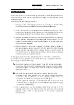
Picture 8.6.2.2.  Input terminals 

Left: MC08122 
Middle: MC09022 
Right: MC10022 

8.7 Connectors 
 

Check connectors and pay attention mainly on possible corrosion, light arc 
marks and the proper tightening torque. Refer torque specifications in 
appendix 17.3. 

8.8 NTC resistor 
 

NTC resistor is mounted to heat sink by using metal glue. In multiple block 
units each block has its own temperature measurement and NTC resistor. For 
fault tracing the resistance values can be found in separate section, (17). 

8.9 Main circuit diagrams 

 
The copies main circuits are attached to the end of this section. The main 
circuit diagrams are presented by frame sizes and voltages.  
 
The CX4 and CX5 main circuits are exactly same for both voltages. The CX2 
main circuit is same for all power sizes of the CX2 -series. The CX6 main 
circuits are presented for all mechanical sizes. 


Summary of Contents for CX

Page 1: ......

Page 2: ...mpting to service repair measures make sure that unit at repair is not powered up if not intended to be Make sure there are no remaining dangerous voltages in circuitry and there is no other voltage source for life threatening dangerous potentials Make sure environment you are working at is safe and won t cause increased risk for personal injury damages for unit or environment Remember also to fol...

Page 3: ...nual M4 M10 29 12 1999 Page 3 To maintain safe construction designed isolation clearances creepage distances and especially correct operation of the complete drive use only spare parts delivered by Producer All rights reserved by Producer ...

Page 4: ...ere manufacturer recommends doing such care taking This manual has been prepared to service technician with supposition that basic skills in electricity electronics and power electronics are as a background skills reinforced with factory provided service training The goal has been clarity and completeness with step by step procedures and accurate technical data The service location has to have a s...

Page 5: ...ns and safety notices 20 6 2 2 Capacitors 21 6 2 3 Re forming after long storage period 21 7 TROUBLESHOOTING 23 7 1 General 23 7 2 Fault codes on panel 23 7 2 1 Fault codes possible reasons and checking to be done 23 7 3 Troubleshooting for a defective unit 50 7 3 1 Warnings 50 7 3 2 Checking instructions 50 7 3 2 1 Checking of current measurement circuit 50 7 3 2 2 Checking of IGBTs 53 7 3 2 3 Ch...

Page 6: ...2 Input Terminals 76 8 7 Connectors 77 8 8 NTC resistor 77 8 9 Main circuit diagrams 77 9 PC BOARDS 78 9 1 General 78 9 2 Power board 78 9 2 1 Description 78 9 2 2 Warnings 79 9 2 3 Layouts connectors and signals 79 9 2 4 Schematic diagrams 88 9 2 5 Troubleshooting 88 9 2 6 Gate circuitry 88 9 2 6 1 Description 88 9 2 6 2 Settings of gate resistors 88 9 2 6 3 Voltage related settings on the board ...

Page 7: ...ry 120 9 6 7 Setting of position jumper 121 9 6 8 Replacement of Extender board 121 9 6 9 Spare parts 122 9 7 VDR board 123 9 7 1 Description 123 9 7 2 Layout connectors and wirings 123 10 OPTIONAL BOARDS 124 11 COOLING FANS 126 11 1 General 126 11 2 Main fans 126 11 3 Warnings 126 11 5 Replacement instructions 127 12 FCDRIVE AND FCLOAD SOFTWARE TOOLS 133 13 APPENDIXES 134 13 1 NTC XLS 134 13 2 To...

Page 8: ...as but not limited to loss of production loss of profit malfunctions or incidental damages of system used with the Products In no event and under no circumstances shall the manufacturer be liable for damages and failures due to misuse abuse improper installation or abnormal conditions of ambient or failures due to operation above rated capacities The manufacturer carries no responsibility for dama...

Page 9: ...r service purposes for fast response of service calls The stock of the spare should be at least one the biggest power size unit of all mechanical sizes in range up to 90kW M7 Producer will compensate stock of spare units in case of unit under manufacturer s warranty has been delivered to replace of the defective unit 4 2 2 Stock of spare parts Service locations will store spare parts based on unit...

Page 10: ... Sensors AC choke Rectifier IGBT Inverter Brake resistor if optional brake chopper is installed Input EMC filter CXL CXS model standard in CXS model Output EMC filter reactor smoothens ripple current and extends service life of DC capacitors The line reactor is desired component in circuitry to reduce harmonic content produced by the rectifier Precharging circuitry Precharging resistor limits surg...

Page 11: ...es for IGBTs in the inverter Gates of the IGBTs are pulsed with 15V Negative pulse is important to achieve proper blocking of the IGBT Complete and proper blocking of the IGBT in case of detected fault current is required The motor and application control block This is software based function where motor is controlled through blocks Motor control ASIC Gate drivers IGBT inverter according actual va...

Page 12: ...4 7nF capacitor and 1Mohm resistor network If needed I O Control board can be bold grounded by jumper X4 on the board 5 2 Technical data 5 2 1 Power ratings Power ratings of the CX L units can be found from the chapter Technical data of the CX CXL CXS user manual 5 2 2 Technical specifications ...

Page 13: ...urrent 2 5 x ICT 2 s every 20 s if output frequency 30 Hz and if the heat sink temperature 60 C 1 5 x ICT for types 90CX4 5 and 90CXL4 5 160CX4 5 and 160CXL4 5 250CX4 5 and 250CXL4 5 400 CX4 5 and 400 CXL4 5 Output frequency 0 500 Hz Frequency resolution 0 01 Hz Control Control method Frequency Control U f characte Open Loop Sensorless Vector Control ristics Closed Loop Vector Control Switching fr...

Page 14: ...ls EN50082 1 2 EN61800 3 Emissions x x CX x x x N x series equipped with external RFI Filter x RFI x x x fulfils EN50081 2 EN61800 3 x x CXL x x x I x series fulfils EN50081 2 EN61800 3 x x CXL x x x C x series fulfils EN50081 1 2 EN61800 3 Safety Fulfils prEN50178 C UL and EN60204 1 CE UL C UL FI COST R check from the namaplate specified approvals for each unit Control Analogue voltage 0 10V Ri 2...

Page 15: ... 35x Un Undervoltage protection Trip limit 0 65 x Un Earth fault protection Protects the inverter from an earth fault in the output motor or motor cable Mains supervision Trip if any of the input phases is missing Motor phase supervision Trip if any of the output phases is missing Unit over temperature Yes protection Motor overload Yes protection Stall protection Yes Motor under load Yes protectio...

Page 16: ...ous voltages entering from the wiring of process control before further measures Remember always to follow local national safety rules and regulation 5 3 2 ESD precautions Electrostatic discharge ESD may destroy electronic components based on MOS or comparable technology IGBT is voltage controlled component and is sensitive for excessive voltages cross gate emitter and gate collector junctions Com...

Page 17: ...p 1000A ac rms signal output 3 Soldering station Soldering desoldering 4 Adjustable power supply 0 1300Vdc 1A adjustable current limit 5 Adjustable power supply 0 690Vac 10 10A three phase galvanic isolation 6 Multimeter Digital portable 7 Insulation tester 1000Vdc 8 Test adapter For gate signal measurement 9 Test adapter By passing of feedback signal 10 Torque wrench 1 12Nm 11 Torque wrench 6 50N...

Page 18: ...alog low power and high power circuits For this reason all component boards are considered to be as spare parts and only Producer has rights to carry out board level repairs if any In any cases if original spare parts are not used to replace defective ones or repair measures are performed for the component boards by unauthorised person warranty will be revoked Complete spare parts list for order a...

Page 19: ...s ratings recommendations are not taken followed as they should be In these cases regular maintenance should be scheduled to guarantee long trouble free service life of the drive In cases if the specifications ratings recommendations are not followed as they should be regular maintenance should be scheduled to guarantee long and trouble free service life of the drive The regular maintenance and in...

Page 20: ... at is safe and won t cause increased risk for personal injury damages for unit or environment Remember also to follow local national safety rules and regulation Internal components and circuit boards are at mains potential when the frequency converter is connected to the mains This voltage is extremely dangerous and may cause death or severe injury if you come contact with it Terminals for the pr...

Page 21: ...complete units are stored without voltage applied for example in sales stock or as a spare units in the factory the re forming of the capacitors should be done at least 12 month period by connecting the voltage into unit and keep unit powered minimum 1 h If the storing time is much longer than a year since unit was energized last time the re forming of the capacitors have to be done in a way that ...

Page 22: ...voltage is set up to rated value of capacitors The degree of re forming process can be then followed by indication of the current meter of the DC power supply It is still recommended to keep voltage at least 1 h even that leakage current is already stabilized earlier Note Due high leakage resistance the dangerous voltage can remain in capacitors long time Discharge capacitors by using resistors af...

Page 23: ...ribed in section 7 The trouble shooting and testing for main circuit and control circuits are described separately in the sections where particular blocks are under consideration 7 2 Fault codes on panel Drive has a capacity to save last nine 9 fault codes and show them on display of control panel if desired There is always a reason or another for the tripping of the drive and it should be solved ...

Page 24: ...ettings OK Disconnect motor cable from the drive Start up the drive Fault was generated by external factor Check motor motor cable features of the load Check the current measuring circuit according to instructions on section 7 3 2 1 Replace defective parts as recommended in spare part lists Clear fault memory F1 Start up the drive F1 NO YES NO YES YES NO ...

Page 25: ...d value on page v7 Fault was generated by external factor line voltage 10 voltage spikes on line feature of load decleration time too short for system inertia break resistor too small Check the voltage measuring circuit according to instructions on section 7 3 2 4 Replace defective parts as recommended in spare part lists Make corrective measures to quality of line power setting the deceleration t...

Page 26: ...otor cable from the drive Start up the drive Fault was generated by external factor damage in insulation of motor cable damage in motor insulation Check the current measuring circuit according to instructions on section 7 3 2 1 Replace defective parts as recommended in spare part lists Clear fault memory F3 Start up the drive F3 NO YES NO YES YES Make corrective measures NO ...

Page 27: ...ard according to instruction 9 2 7 Power and start up the drive Run through the frequency range Fmin Fmax Check the gate drive circuits according to instructions on section 7 3 2 3 Replace defective parts as recommended in spare part lists Clear fault memory F4 Check IGBT according to instructrions on section 7 3 2 2 F4 Please follow the procedures described in F5 troubleshooting section NO YES NO...

Page 28: ...ARGING SWITCH Replace the control board with functional one by following instructions on section 9 3 6 Replace defective parts as recommended on spare parts list Load software into the control board by using FCload Clear fault memory Set values of parameters to comply with nature of application F5 YES NO ...

Page 29: ...o monitored value on page v7 Fault was generated by external factor line voltage 15 of nominal set by parameter line dips features of the load blown input fuses Or internal factor faulty rectifier Check the voltage measuring circuit according to instructions on section 7 3 2 4 Replace defective parts as recommended and listed in spare part lists Clear fault memory NO YES Actual value Monitored val...

Page 30: ...lt memory Check voltage on input phases Voltage line setting of 1 14 Occasionally existing line dips or disturbances may activate line supervision function Ensure quality of line power Check condition and operation of charging contactor Check control signal for charging switch according to instructions on section 7 3 2 6 Check that jumper X1 is in its place on the power board F10 F10 Replace the c...

Page 31: ...m drive to motor F11 OUTPUT PHASE SUPERVISOR Check operation of the current measuring circuit according to instructions on section 7 3 2 1 Replace defective parts as recommended and listed in spare parts lists Clear fault memory Connections OK Make corrective measures to circuit from the drive to motor NO YES ...

Page 32: ...k conditions of IGBT in the Dynamic Braking Chopper according to instructions on section 7 3 2 5 Replace power board according to instructions on section 9 2 7 Clear fault memory Circuit OK Make corrective measures Check the dimensioning of the braking resistor NO YES IGBT s OK Replace defective IGBT s according to instructions on section 8 4 4 F12 NO YES YES NO ...

Page 33: ...TROUBLESHOOTING Service Manual M4 M10 11 07 2002 Page 33 ...

Page 34: ...TROUBLESHOOTING Service Manual M4 M10 11 07 2002 Page 34 ...

Page 35: ... versus rating of the motor and the drive Combination of the rating for motor and drive do not match with mechanical load Clear fault memory F15 Measure actual motor current and compare it to value on monitoring page v3 Measured current Monitored current Check the current measuring circuit according to instructions on section 7 3 2 1 Replace defective parts as recommended in spare part lists NO YE...

Page 36: ...d current Dimensioning of the motor too low Measure temperature of the motor and compare to value on monitoring page n20 calculated motor temp 105 Trip limit Check the current measuring circuit according to instructions on section 7 3 2 1 Replace defective parts as recommended in spare part lists F16 If cooling of the motor is ok then there is drive overcurrent or motor temperature is lower than r...

Page 37: ...g to requirements of application F17 MOTOR UNDER LOAD Measure motor current and compare result to value on monitoring page v3 Check the current measuring circuit according to instructions on section 7 3 2 1 Replace defective parts as recommended in spare part lists Clear fault memory t measured t monitored NO YES ...

Page 38: ...T HARDWARE FAULT Disconnect control from the input terminals 4 and 5 Clear fault memory F18 F18 Replace the control board with functioning one according to instructions on section 9 3 6 Load software into Control board according to instructions on section 12 and set parameters Measure signal level in current loop Value 0 20mA Make corrections to external control circuit F18 YES YES NO NO NO YES YE...

Page 39: ... IDENTIFICATION Clear fault memory Voltage OK Replace the optional board with functioning one according to optional board users manual s instrucions Check on operation voltage of the optional board from the connector X1 X2 X6 for 12V 24V Check power feeding lines from power board to optional board for bad connections F19 YES NO NO YES ...

Page 40: ...re voltage across terminals 1 3 on control board Clear fault memory 10V ref OK 10V ref OK Replace the control board with functioning one according to instructions on section 9 3 6 Load software into Control board according to instructions on section 12 and set parameters Reference signal is loaded excessively by external circuit Iout 10mA Make corrective measures to external control circuit YES NO...

Page 41: ...control board Clear fault memory 24V source OK Replace control board with functioning one according to instructions on section 9 3 6 Replace defective parts as recommended in spare part lists Load software into Control board according to instructions on section 12 and set parameters 24V source is loaded excessively by an external circuit Iout 100mA Make corrective measures to external control circ...

Page 42: ...pply shuts down Change value of some parameter and press ENTER Disconnect input power F22 F23 Replace control board with functioning one according to instructions on section 9 3 6 Replace defective parts as recommended in spare part lists Load software into the control board according to instructions on section 12 Power up the drive F22 F23 Power up the drive F22 F23 YES NO NO YES YES NO ...

Page 43: ...tart up the unit F25 MICROPROCESSOR WATCH DOG Clear fault memory Replace the control board with functioning one according to instructions on section 9 3 6 Replace defective parts as recommended in spare part lists Load software into Control board according to instructions on section 12 and set parameters ...

Page 44: ...COMMUNICATION Clear fault memory F26 Replace the control board with functioning one according to instructions on section 9 3 6 Replace defective parts as recommended in spare part lists Load software into Control board according to instructions on section 12 and set parameters Plug functional panel in place YES NO ...

Page 45: ...ring OK Thermistor OK Short terminals 21 22 on optional board Replace option board with functioning one according to instructions in option board s users manual Replace defective parts as recommended in spare part lists Replace the termistor F29 F29 YES YES NO YES Make corrections to wiring F29 Fault activated by external factor Check external circuit and thermistor NO NO NO NO YES YES Check tempe...

Page 46: ...h functioning one according to instructions on section 9 3 6 Replace defective parts as recommended in spare part lists Make corrective measures to external control circuit I 4mA Measure actual value of signal in current loop Actual value Monitored value Load software into Control board according to instructions on section 12 5 3 and set parameters YES YES NO NO ...

Page 47: ...rol board with functioning one according to instructions on section 13 4 2 Replace defective parts as recommended in spare part lists Fault activated for purpose Read status of programmable input from monitoring page v15 Actual status Monitored status Load software into control board according to instructions on section 12 5 3 and set parameters NO YES ...

Page 48: ...oftware again Turn off the power wait and start up the drive Clear fault memory AC ON NO YES AC ON Replace the control board with operative one according to instructions on section 9 3 6 Replace defective parts as recommended in spare part lists Possible interference of control signals or RS232 cablel Load software into the control board according to instructions 12 and set parameters NO NO YES YE...

Page 49: ...PH supply PANEL DEAD DC link voltage AC DC rectifier or charging circuit faulty Check serial communication connections and panel Power supply running External overload of 24V output or power supply failure Replace power board according to instructions on section 9 2 7 NO NO YES YES ...

Page 50: ... CXL5 up to 90 kW CX6 up to 75 kW Passive checking While unit unpowered check resistance values of shunt resistors on Adapter boards CB00005 CB00009 For location of the shunt resistors R4 R9 look at layout drawing of the particular type of the board in section PC BOARDS Functional checking While the unit is powered up but not running measure voltage level from connector X2 pins 6 7 8 on Control bo...

Page 51: ...To power up the drive under investigation disconnect wire harness from connector X8 on Power boards Connect lead from terminal of the external power supply to connector X8 1 on the Power board and respectively terminal of the external power supply to negative bus of the drive With new power board CB00042 CB00055 layout it is possible to disconnect DC from main circuit by pulling jumper X22 off and...

Page 52: ...se signal recommended otherwise earth fault occurred set protection function temporarily off parameter 7 4 Measure signals from Control board terminal X2 pins 6 7 and 8 to DC Value of the signals at terminal X2 shall be as follows M8 U X2 1 2 U X5 X6 M9 U X2 1 3 U X5 X6 M10 U X2 1 4 U X5 X6 Look at value on monitoring display n3 motor current and compare it to nominal rated current constant torque...

Page 53: ... visible checking cannot be judged to be failed advanced techniques have to be used Threshold voltage checking To check condition of IGBTs digital multimeter with diode checking mode is needed Line and motor leads disconnected measure threshold voltages cross CE junctions of the IGBTs according instructions as in section 8 2 3 AC TO DC CONVERTER Checking of gate capacitance Remember ESD protection...

Page 54: ...t powered At connector X3 on the Control board pins 2 4 8 10 and 14 16 will be connected together to bypass feedback signal from the IGBTs This has to be done to avoid fault F4 at start up and to be able to measure gate signals while control circuitry is operating only With frame sizes M4 to M7 use extended connector between control board and power board pins are too short to add jumper 2 4 8 10 1...

Page 55: ... to connector X21 on the Power board and respectively terminal of the external power supply to negative bus of the drive NOTE It is important to disconnect wire harness or jumper X22 from each Power board Otherwise DC bus will charge up trough not disconnected power board When circuit boards are powered measure DC bus voltage that it is zero The unpowered main circuit reduces risks for destructive...

Page 56: ...ic in time and level shall be in range 15V 12V Positive level of the gate signal shall remain within 14 5 15 5 V in one bay units and respectively 14 9 15 1 V in units constructed in multiple bays M8 to M10 Figure 7 4 Gate pulses Existence of the negative signal is very important for reliable operation of IGBT especially in situations where IGBT should be able to block down high collector current ...

Page 57: ...r that voltage from connector X15 13 on Power board Voltage level as above in accordance with nominal voltage rating of the unit If the voltage is out of tolerance 1 reason for the malfunction is failure on the Power board and it has to be replaced as instructed in section 9 2 7 Otherwise excessive load by the Control board is pulling down the signal and is indication of failure on the Control boa...

Page 58: ...er board s board by board If voltage level variates from values above 3 58V 3 70V 3 58V at connector particular Power board is defective and has to be replaced according to instructions in section 9 2 7 Otherwise failure can be suspected to be on one of the Extender board in unit 7 3 2 5 Checking of braking chopper Check parameter 4 5 to enable brake chopper function p4 5 1 Visual checking At the ...

Page 59: ...eling diode in braking chopper Configuration of main terminals variates depending on construction For detailed specification of connections consult the USER s MANUAL delivered with device The CE junction of the IGBT will be checked by DMM in diode mode Shorted CE junction results value zero for threshold voltage checking measured in both direction At the measurement terminal R of the braking resis...

Page 60: ... the chapter 8 3 operation and troubleshooting of the main circuit 7 3 2 7 Checking of rectifiers See the chapter 8 2 3 for troubleshooting 7 3 2 8 Checking of DC bus capacitors To check DC bus capacitors external adjustable DC power supply is needed Functional checking Charge up DC capacitors one by one slowly up to nominal voltage of component and check leaking current Value of leakage current s...

Page 61: ...ier The rectifier is either module including six diodes three individual modules including two diodes or alternatively in semi controlled bridge one diode and one SCR per module in phase The line reactor is wound to common core for optimised inductance value with high enough saturation point in compact mechanical size Diode or semiconductor bridge is module type component installed onto heat sink ...

Page 62: ...junctions When diode biased forward resistance value should be in range 10kohm 100kohm and threshold voltage around 0 5V cross the PN junction if diode is not damaged Value in resistance mode variates depending on source voltage and internal impedance of the multi meter therefore it is recommended to use diode checking mode Reverse biased PN junction diode should give values as infinite in either ...

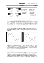
Page 63: ...r K1 instead of input terminals Notify proper location and order of the terminals When a drive is powered up by the three phase line and the drive is running and loaded the shape of current drawn from the input phase looks as figures 8 3 and 8 4 Figure 8 3 High inductive reactance Figure 8 4 Lower inductive reactance On figure 8 3 inductive reactance is higher than on figure 8 4 Higher reactance i...

Page 64: ... by the function of the input phase supervision voltage level in DC bus is rectified from two phases to charge DC capacitors to level Udc Uin 0 9 when rectifier is loaded The rectification factor 0 9 is result of two phase four pulse rectifier and matches with formula 0 9 4 2 2 π Design and rating of DC link supports ripple in range of 270 396Hz with hold up capacity accordingly to ripple generate...

Page 65: ...r thermal junction from semiconductor to the heat sink 5 Clean base plate of the semiconductor by sweeping it the first with ethanol damped clean rag and after that with clean dirt free dry rag 6 Before installation make sure that screws for fastening are in good condition and length is correct and check the base plate of the semiconductor from damages especially on the base plate 7 Apply fresh th...

Page 66: ...n table TORQ XLS in section 17 Follow the information on column TORQUE 2 3 The third and final tightening again in the order as above in phases 1 and 2 The specification for torque is in table TORQ XLS in section 17 Follow the column TORQUE FINAL 8 2 6 Wiring table Wiring of front end is following next order of connections Terminal L1 Line reactor Rectifier L1 Terminal L2 Line reactor Contactor or...

Page 67: ...oth and stable DC energy for a PWM inverter Stable voltage in DC bus is required for proper high performance operation with topology of voltage source inverter Negative feature of the DC capacitors is internal leakage current through insulation layer which variates some amount from individual capacitor to another This feature causes variation in voltages divided cross the serial connected capacito...

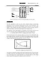
Page 68: ...via resistor s until energy in DC bus has rosen on the level which corresponds 85 of nominal dc voltage level Unominal AC 1 35 0 85 charging switch will be closed On the next figure 8 8 the charging switch is closed in the moment t1 the precharging resistor is out of circuit and full three phase power is lead to DC bus At the same time t1 circuit becomes low impedance which causes DC voltage to ju...

Page 69: ...forward the value of the voltage should be within range of 0 3 0 5V if resistor is not burned open Phase L1 is lead via charging contactor and value should be infinite If charging switch will not be activated pulled in within few seconds from connection to mains procedure for trouble shooting of failing operations of the charging switch are following 1 Check input phases for missing power If power...

Page 70: ... DC link voltage Pulse lengths are depending on needed motor voltage 8 4 3 Troubleshooting Troubleshooting of IGBTs is described in the section 7 3 2 2 8 4 4 Assembly instructions of IGBTs IGBT is sensitive component for an electro static discharge ESD and shall be handled in any phase of assembly in manner of safe ESD working Wear antistatic clothes as well as antistatic shoes and wrist wrap conn...

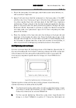
Page 71: ...n by hands to avoid dropping them off Procedure to tighten down the screws will be done in three phases in order to avoid risks of damages by mechanical stress in the module 8 4 5 Tightening order and torque An order to torque down the fastening screws is illustrated on figure below In the case of module with four holes for fastening always start from a long side of the module and circle around th...

Page 72: ...g resistors balance voltages over the series connected electrolytic DC bus capacitors and discharge dangerous voltages within reasonable time when power supply is switched off 8 5 3 Troubleshooting Damaged resistor can normally be inspected visually due in case of overloading the resistors are mechanically broken Resistance values also can be checked by multimeter Refer the measured values to the ...

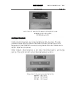
Page 73: ...repair Frame Drawing no M8 690V JS001 M9 690V JS002 M10 690V JS003 Plastic capacitors must be installed clued on top of the DC bus bar between DC and DC Ordered spare bus bar capacitors are already fixed See following images to identify bus bar components Picture 8 6 1 1 MC09039 M9 690V DC bus bar Picture 8 6 1 2 MC10027 M10 690V DC bus bar Picture 8 6 1 3 MC09054 M9 690V DC bus bar with capacitor...

Page 74: ...999 Page 74 Picture 8 6 1 4 MC10033 M10 690V DC bus bar with capacitors Picture 8 6 1 5 MC09034 M9 400 500V DC bus bar with capacitors Picture 8 6 1 6 MC10031 M10 400 500V DC bus bar with capacitors Picture 8 6 1 7 MC9033 M9 L bus bar 400 690V ...

Page 75: ... Manual M4 M10 29 12 1999 Page 75 Picture 8 6 1 8 MC07033 M10 L bus bar 400 690V Picture 8 6 1 9 DC bus bars 400 500V MC09032 M9 lower MC10030 M10 upper Picture 8 6 1 10 MC07013 Bus bar link between DC capacitors 400 500V ...

Page 76: ...en DC bus bars This link combines single DC links parallel Bus bars are used to end of year 1999 Beginning of year 2000 DC terminals are replaced with wider model where all DC wires are connected Older model s interconnection is not done Recommended to add during service This action smooth current sharing between sections Picture 8 6 2 1 Interconnection bus bar for DC MC08158 M8 upper MC01062 M9 m...

Page 77: ... heat sink by using metal glue In multiple block units each block has its own temperature measurement and NTC resistor For fault tracing the resistance values can be found in separate section 17 8 9 Main circuit diagrams The copies main circuits are attached to the end of this section The main circuit diagrams are presented by frame sizes and voltages The CX4 and CX5 main circuits are exactly same...

Page 78: ...ard 9 2 1 Description Power board consists internal power supply based on switching topology Pulse amplifiers for gate control so called gate drivers are located on the Power board also The power board produces electrical energy for internal control circuitry as well as purposes of signals of the process control The power supply is protected from over loading or short circuit in secondary circuitr...

Page 79: ...sformer in switching power supply Isolation level is 2 5kV Any time if intended to be performed testing or repair make sure that techniques which are going to be used complies with general safe working instructions Make sure that equipments used for the tests are designed to voltage levels which can exist in circuit Be awared that additional capacitance of measuring devices may cause an operation ...

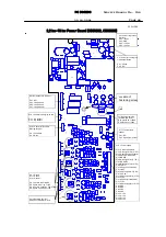
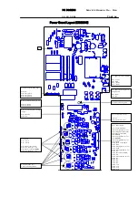
Page 80: ...5 V36 V3 7 V3 8 V39 V40 V41 V42 V43 V4 4 V4 5 V46 V4 7 V48 V49 V5 0 V51 V5 2 V53 V54 V55 V56 V5 7 V58 V59 V60 V6 1 V7 1 V72 V73 X1 X2 X3 X4 X5 X6 X7 X8 X9 X10 X1 1 X1 2 X13 X1 4 X15 X1 6 X17 X1 8 X1 9 Gate Resistors Rx Ry Values on table GATE XLS 2 2 kw 90 kw Power Board CB00002 CB00003 Voltage programming resistors R9 R18 R18 placed on 400V R9 placed on 500V X9 Gate U X11 Gate V X13 Gate W Pin 1 ...

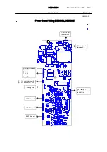
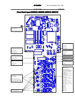
Page 81: ...60 R61 R6 2 R6 3 R64 R65 R66 R67 R68 R69 R71 R72 R73 R74 R75 R76 R77 R78 R79 R80 R81 R82 R83 R84 R85 R8 6 R8 7 R88 R8 9 R9 0 R91 R92 R93 R95 R96 R97 R98 R99 R100 R101 R10 2 R103 R10 4 R105 R10 6 R10 7 R1 08 R1 09 R1 10 R11 1 R112 R116 R117 R11 8 R119 R120 R12 1 R12 2 R12 3 R124 R12 5 R12 6 R16 0 T1 T2 V1 V2 V3 V4 V5 V6 V7 V8 V9 V10 V11 V12 V13 V14 V15 V16 V17 V18 V19 V20 V21 V22 V23 V24 V25 V26 V2...

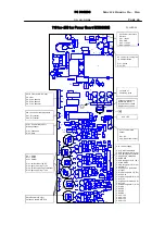
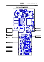
Page 82: ... R1 51 R152 R1 53 R1 54 R1 55 R1 56 R1 57 R1 58 R1 59 R1 60 T1 V1 V2 V3 V4 V5 V6 V7 V8 V9 V1 0 V12 V13 V14 V15 V16 V1 7 V19 V20 V21 V22 V23 V24 V25 V26 V2 8 V2 9 V30 V31 V32 V33 V35 V36 V37 V38 V39 V40 V41 V42 V44 V45 V46 V47 V48 V4 9 V51 V52 V53 V54 V55 V56 V57 V58 V59 V60 V61 X1 X2 X3 X4 X5 X6 X7 X8 X9 X10 X1 1 X12 X13 X14 X15 X1 6 X17 X18 X19 X20 110 kw 250 kw Power Board CB00020 PC20B DS4 Volt...

Page 83: ...0 R 61 R 6 2 R 6 3 R 6 4 R 6 5 R 6 6 R 6 7 R 68 R 69 R 7 0 R 71 R 72 R 73 R 74 R 75 R 76 R 77 R 78 R 79 R 80 R 81 R 82 R 83 R 84 R 85 R 8 6 R 8 7 R 88 R 89 R 9 0 R 91 R 92 R 93 R 9 4 R 95 R 96 R 97 R 9 8 R 99 R 10 0 R 10 1 R 10 2 R 10 3 R 10 4 R 1 05 R 10 6 R 10 7 R 1 08 R 1 09 R 1 10 R 11 1 R 11 2 R 11 3 R 11 4 R 11 5 R 11 6 R 11 7 R 11 8 R 11 9 R 1 2 0 R 12 1 R 1 2 2 R 1 23 R 12 4 R 12 5 R 12 6 ...

Page 84: ...6 H7 H8 H9 H10 H11 H12 H13 H14 H15 H16 H17 K1 K2 K3 Q1 Q2 R1 R2 R3 R4 R5 R6 R7 R8 R9 R10 R11 R12 R13 R14 R15 R16 R17 R18 R19 R20 R21 R22 R23 R24 R25 R26 R27 R28 R29 R30 R31 R32 R33 R34 R35 R36 R37 R38 R39 R40 R41 R42 R43 R46 R47 R48 R49 R50 R51 R52R53 R54 R55 R56 R57 R58 R59 R60 R61 R62 R63 R64 R65 R66 R67 R70 R71 R72 R73 R74 R75 R76R77 R78 R79 R80 R81 R82 R83 R84 R85 R86 R87 R88 R89 R90 R91 R94 R...

Page 85: ...10 R11 R12 R13 R14 R15 R16 R17 R18 R19 R20 R21 R22 R23 R24 R25 R26 R27 R28 R29 R30 R31 R32 R33 R34 R35 R36 R37 R38 R39 R40 R41 R42 R43 R46 R47 R48 R49 R50 R51 R52R53 R54 R55 R56 R57 R58 R59 R60 R61 R62 R63 R64 R65 R66 R67 R70 R71 R72 R73 R74 R75 R76R77 R78 R79 R80 R81 R82 R83 R84 R85 R86 R87 R88 R89 R90 R91 R94 R95 R96 R97 R98 R99 R100 R101 R102 R103 R104 R105 R106 R107 R108 R109 R110 R111 R112 R1...

Page 86: ... 150 R 151 R152 R153 R 154 R155 R156 R 157 R 158 R159 R160 R161 R 162 R 163 R 164 R 165 R 166 R167 R 168 R 169 R 170 R 171 R 172 R 173 R 174 R 175 R 176 R 177 R 178 R179 R 180 R 181 R 182 R 183 R 184 R 185 R186 R 187 R 188 R 189 S 1 T 1 T 2 V 1 V 2 V 3 V 4 V 5 V 6 V 7 V 8 V 9 V 10 V 11 V 12 V 13 V 14 V 15 V 16 V 17 V 18 V 19 V 21 V 22 V 23 V 24 V 25 V 26 V 27 V 28 V 29 V 30 V 31 V 32 V 33 V 34 V 3...

Page 87: ... H20 H21 K1 K2 K3 Q1 Q2 R1 R2 R3 R4 R5 R6 R7 R8 R9 R10 R11 R12 R13 R14 R15 R16 R17 R18 R19 R20 R21 R22 R23 R24 R25 R26 R27 R28 R29 R30 R31 R32 R33 R34 R35 R36 R37 R38 R39 R40 R41 R42 R43 R44 R45 R46 R47 R48 R49 R50 R51 R52 R53 R54 R55 R56 R57 R58 R59 R60 R61 R62 R63 R64 R65 R66 R67 R68 R69 R70 R71 R72 R73 R74 R75 R76 R77 R78 R79 R80 R81 R82 R83 R84 R85 R86 R87 R88 R89 R90 R91 R92 R93 R94 R95 R96 R...

Page 88: ... level 0 5V pulses to 15V pulses for gates of IGBTs in inverter section While the gate amplifier is feeding pulses in regulated levels charging time of gate junction can be considered as a capacitor is controlled by gate resistors according to rating of the IGBT in particularly rated drive Proper control for IGBTs are required to achieve lowest possible internal losses such as switching losses and...

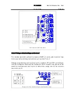
Page 89: ...n 2 gate lower leg 15V Pin 4 emitter upper leg FLOATING Pin 5 gate upper leg 15V 1 2 4 5 Gate resistors on the Power board 9 2 6 3 Voltage related settings on the board For reliable operation with various types of IGBTs in units gate resistors have to be selected according instructions as in section 9 2 6 2 Voltage programming will be done by the resistors R9 and R19 according to nominal voltage t...

Page 90: ...on layout drawings of the Power boards Below is a partial picture of the board to locate position of the fastening screw C14 C15 C16 C 2 2 C 2 3 C 2 4 C 2 5 C 26 C 2 7 C 48 C52 D 9 D 1 1 D 1 3 H 18 R 7 R 9 R 10 R 13 R 1 8 R 72 R 102 R109 R110 R 111 R 119 V59 V60 X 1 X 5 X 6 X 7 X8 X19 Voltage programming resistors R9 R18 R18 placed on 400V R9 placed on 500V 1 3 5 7 1 2 1 X1 Location of Fastening s...

Page 91: ... the board all firmware as well as parameter values are stored into memory chips The Control board provides isolation from main circuit to process interface The plug in terminals for the process control are placed on the board Multi layer technique is used in design of artwork of the board The SMD components are the mostly used on the board for high density design Digital inputs Configured in two ...

Page 92: ...5ms Open collector output 48V maximum Current capacity 50mA max to be cut off 9 3 2 Warnings The Control board is connected via board to board connector to Power board which is on potential of DC bus and carries dangerous energies Any time if intended to be performed testing or repair make sure that techniques which are going to be used complies with general safe working instructions of an electri...

Page 93: ...ly Pin1 Current disbalance Pin2 Gate signal UH 0 5V Pin3 Charging switch control Pin4 Phase U status PHU Pin5 BRKFB Pin6 Gate signal UL 0 5V Pin7 BRKDRV Pin8 Gate signal VH 0 5V Pin9 TEMP Pin10 Phase V status PHV Pin11 NET Pin12 Gate signal VL 0 5V Pin13 UCIN Pin14 Gate signal WH 0 5V Pin15 8V Pin16 Phase W status PHW Pin17 8V Pin18 Gate signal WL 0 5V Pin19 DC Pin20 DC Pin21 DC Pin22 DC Pin23 15V...

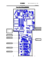
Page 94: ... V43 V44 V4 5 V4 6 V4 7 V48 V49 V5 0 V51 V52 V53 V5 4 V5 5 V56 V57 V58 V59 V6 0 V61 V62 V63 V6 4 V6 5 V66 V6 7 V6 8 V6 9 V7 0 V71 V7 2 V7 3 V7 4 V7 5 V7 6 V7 7 V7 8 V79 V8 0 V81 V8 2 V83 V8 4 V8 5 V86 V8 7 V1 01 V1 02 W1 X7 X8 X9 X1 0 X1 3 1 2 3 4 5 6 7 8 9 10 11 12 13 14 15 16 17 18 19 20 21 22 23 24 25 26 1 1 1 1 WIRE01 DS4 NOTE Terminals X2 X3 and X14 are in potential of negative DC bus DANGER ...

Page 95: ...of process interface can be checked by monitoring statuses of inputs and outputs on display as well as analog signals on input and output terminals 9 3 6 Replacement of Control Board 1 Make sure unit is unpowered and possibly used bypass circuit does not feed back energies to the drive 2 Remove a control panel from bracket by squeezing the locking clips on both sides of the panel to direction of c...

Page 96: ...cal constructions M4 and M5 particular plate to connect GND of process cabling is fastened on the Control board and it has to be removed Grounding plate 6 Disconnect all control cables from connectors of the Control boards 7 Pull out board to board pin connector 2 13 pins from female socket Be very careful to avoid bend pins out of line 8 Remove a fastening screw to release the Control board Locat...

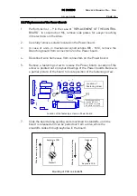
Page 97: ...e the standoffs slides through keyholes in the board Standoff Keyhole in PCB Slide the board up for releasing Slide the board down for locking Keyhole in PCB Standoff Mounting of PCB on standoffs 11 Before to assemble a new Power board into the drive do all the required settings to the board according to instructions in section 9 2 6 Assemble the board into drive in reversed order of the procedure...

Page 98: ...tional current signal is converted to voltage signal for the further processions The CT modules are placed either on the Adapter board or mounted on chassis of the drive Resistors in current measurement circuitry for type of the drive related settings are placed on the board The resistor settings are specified on chart CX2ADAP XLS CX4ADAP XLS and CX6ADAP XLS and described in section 17 Precharging...

Page 99: ...ia connector X11 X7 From Power Board Pin1 GND Pin2 26Vdc X8 Relay Pin1 GND Pin2 26Vdc X9 Fan_1 Pin1 GND Pin2 24Vdc X10 Fan_2 Pin1 GND Pin2 24Vdc X11 Fan Control Pin1 26Vdc Pin2 X9 2 X10 2 X1 Charge Pin1 Contactor K1 1 Pin2 Contactor K1 2 X2 Discharge Pin1 DCM Pin3 DC Pin5 DC X6 From Power Board Pin1 Current signal IWIN Pin2 Current signal IVIN Pin3 Current signal IUIN Pin4 DC Pin5 DC Pin6 DC NOTE ...

Page 100: ... 1 1 1 1 1 1 1 1 WIRE5 DS4 Wiring of Adapter Board M4 CB00005 NOTE Terminals X1 X2 and X6 are in high potential DANGER WARNING Power board terminal X2 Fan_2 Charging switch External control for fans Fan_1 Control board terminal X2 Capacitor bank 1 midle point 3 DC 5 DC 1 Charging switch 2 Power board terminal X19 2 ...

Page 101: ...ctor K1 2 X11 Fan control Pin1 26Vdc Pin2 X9 2 X10 2 X7 From Power Board X1 GND X2 26Vdc W1 Jumper Placed on Continuous power for fans Removed Controlled power for fans via connector X11 X10 Fan_2 Pin1 GND Pin2 24Vdc X9 Fan_1 Pin1 GND Pin2 24Vdc Current sensors 7 5 11kW Type 50A 15kW Type 100A NOTE Terminals X1 and X6 are in high potential DANGER WARNING X6 From Power Board Pin1 Current signal IWI...

Page 102: ... R R R R1 R1 R1 W1 X1 X6 X7 X9 X1 X11 1 1 1 1 Wiring of Adapter Board M5 CB00006 CB00009 WIRE6 DC4 NOTE Terminals X1 and X6 are in high potential DANGER WARNING Contactor terminals 1 2 Power board terminal X2 Fan_1 Fan_2 Control board terminal X2 External control for fans ...

Page 103: ...aced on Continuous power for fans Removed Controlled power for fans via connector X11 X11 Fan control Pin1 26Vdc Pin2 X9 2 X10 2 X10 Fan_2 Pin1 GND Pin2 24Vdc X9 Fan_1 Pin1 GND Pin2 24Vdc Precharging resistors CB00007 3pcs placed on CB00008 4pcs placed on NOTE WARNING X4 To Expander board Pin1 15Vdc Pin2 Common U Pin3 Common V Pin4 Common W Pin5 15Vdc Pin6 Current signal IU Pin7 Current signal IV ...

Page 104: ...R13 W1 X X X X X X1 X1 1 1 1 1 1 Wiring of Adapter Board M6 M10 CB00007 and CB00008 WIRE7 DS4 NOTE Terminals X1 X4 and Precharging resistors are in high potential DANGER WARNING Current transducers Expander board terminals X5 or X6 Charging switch Power board terminal X2 Fan_1 Fan_2 External control for fans ...

Page 105: ...2ADAP XLS CX4ADAP XLS and CX6ADAP XLS in section 17 For location of the resistors look at layout drawings of the Adapter boards in section 9 4 3 9 4 7 Settings on board Any time if the Adapter board has failed and will be replaced with a spare board type related settings of the current measuring circuit have to be done The spare board are not equipped with the scaling resistors by manufacturer For...

Page 106: ...The branching board is connected to potential of DC bus and carries dangerous energies to be touched 9 5 3 Layout connectors and wiring Layout drawing connectors and wiring of the Branching board is illustrated on next page X1 X2 X3 X4 Branching Board CB00018 PC18B DS4 ...

Page 107: ...OARDS Service Manual M4 M10 22 10 2001 Page 107 X1 X X3 X Branching Board CB00018 PC18B DS4 To Expander board terminal X2 To Control Power boards via board to board connector To Expander board terminal X10 ...

Page 108: ...nals are delayed on the boards for simultaneous gating of the IGBTs Due to relatively long signal transmission line signal clarity and signal proneness are coming to be an issue To achieve proper signal existence such as levels and proper timing signal is filtered buffered and delayed on the Extender board Currents measured from the each output phases of each blocks are processed on the Extender b...

Page 109: ...rcuit the board is connected to DC potential for reference to functions and measurements For this reason the board carries dangerous high voltages 9 6 3 Layout connectors and wirings Layout drawing of the Extender board with descriptions of settings in current measuring circuit and location the jumpers are described on following page ...

Page 110: ... R55 R56 R57 R58 R59 R60 R61 R62 R63 R64 R6 5 R66 R67 R6 8 R6 9 R7 0 R7 6 R7 7 R8 0 R86 R9 0 R91 R94 R95 R9 6 R9 9 R1 00 R1 01 R1 03 R104 R105 R1 06 R1 07 R1 08 R1 09 R1 10 R1 11 R1 12 R113 R114 R1 15 R1 16 S1 S2 S3 T1 T2 T3 T4 V1 V2 V3 V4 V5 V6 V7 V8 V9 V1 0 V11 V1 2 V13 V14 V15 V16 V1 7 V18 V1 9 V2 0 V21 V22 V2 3 V24 V42 X2 X3 X4 X5 X6 X7 X8 X9 X1 0 X1 1 Expander Board CB00019 PC19C DS4 Location...

Page 111: ...4 R85 R86 R87 R88 R89 R90 R91 R92 R93 R94 R95 R96 R97 R98 R99 R100 R101 R102 R103 R104 R105 R106 R107 R108 R109 R110 R111 R112 R113 R114 R115 R116 R117 R118 R119 R120 R121 R122 R123 R124 R125 R126 R127 R128 R129 R130 R131 R132 R133 R134 R135 R136 R137 R138 R139 R140 R141 R142 R143 R144 R145 R146 R147 R148 R149 R150 R151 R152 R153 S1 S2 S3 S4 S5 S6 S7 S8 S9 S11 T1 T2 T3 T4 V1 V2 V3 V4 V5 V6 V7 V8 V...

Page 112: ...3 R84 R85 R86 R87 R88 R89 R90 R91 R92 R93 R94 R95 R96 R97 R98 R99 R100 R101 R102 R103 R104 R105 R106 R107 R108 R109 R110 R111 R112 R113 R114 R115 R116 R117 R118 R119 R120 R121 R122 R123 R124 R125 R126 R127 R128 R129 R130 R131 R132 R133 R134 R135 R136 R137 R138 R139 R140 R141 R142 R143 R144 R145 R146 R147 R148 R149 R150 R151 R152 R153 S1 S2 S3 S4 S5 S6 S7 S8 S9 S11 T1 T2 T3 T4 V1 V2 V3 V4 V5 V6 V7 ...

Page 113: ... R84 R85 R86 R87 R88 R89 R90 R91 R92 R93 R94 R95 R96 R97 R98 R99 R100 R101 R102 R103 R104 R105 R106 R107 R108 R109 R110 R111 R112 R113 R114 R115 R116 R117 R118 R119 R120 R121 R122 R123 R124 R125 R126 R127 R128 R129 R130 R131 R132 R133 R134 R135 R136 R137 R138 R139 R140 R141 R142 R143 R144 R145 R146 R147 R148 R149 R150 R151 R152 R153 S1 S2 S3 S4 S5 S6 S7 S8 S9 S11 T1 T2 T3 T4 V1 V2 V3 V4 V5 V6 V7 V...

Page 114: ...3 R84 R85 R86 R87 R88 R89 R90 R91 R92 R93 R94 R95 R96 R97 R98 R99 R100 R101 R102 R103 R104 R105 R106 R107 R108 R109 R110 R111 R112 R113 R114 R115 R116 R117 R118 R119 R120 R121 R122 R123 R124 R125 R126 R127 R128 R129 R130 R131 R132 R133 R134 R135 R136 R137 R138 R139 R140 R141 R142 R143 R144 R145 R146 R147 R148 R149 R150 R151 R152 R153 S1 S2 S3 S4 S5 S6 S7 S8 S9 S11 T1 T2 T3 T4 V1 V2 V3 V4 V5 V6 V7 ...

Page 115: ...84 R85 R86 R87 R88 R89 R90 R91 R92 R93 R94 R95 R96 R97 R98 R99 R100 R101 R102 R103 R104 R105 R106 R107 R108 R109 R110 R111 R112 R113 R114 R115 R116 R117 R118 R119 R120 R121 R122 R123 R124 R125 R126 R127 R128 R129 R130 R131 R132 R133 R134 R135 R136 R137 R138 R139 R140 R141 R142 R143 R144 R145 R146 R147 R148 R149 R150 R151 R152 R153 S1 S2 S3 S4 S5 S6 S7 S8 S9 S11 T1 T2 T3 T4 V1 V2 V3 V4 V5 V6 V7 V8 ...

Page 116: ...3 R84 R85 R86 R87 R88 R89 R90 R91 R92 R93 R94 R95 R96 R97 R98 R99 R100 R101 R102 R103 R104 R105 R106 R107 R108 R109 R110 R111 R112 R113 R114 R115 R116 R117 R118 R119 R120 R121 R122 R123 R124 R125 R126 R127 R128 R129 R130 R131 R132 R133 R134 R135 R136 R137 R138 R139 R140 R141 R142 R143 R144 R145 R146 R147 R148 R149 R150 R151 R152 R153 S1 S2 S3 S4 S5 S6 S7 S8 S9 S11 T1 T2 T3 T4 V1 V2 V3 V4 V5 V6 V7 ...

Page 117: ...1 7 V1 8 V1 9 V2 0 V 21 V2 2 V 23 V2 4 V4 2 X2 X 3 X4 X5 X6 X7 X8 X9 X10 X11 A1 A 2 A3 A 4 A 5 A1 0 A1 1 A1 2 A 13 A2 5 A 30 A 31 A3 2 B 1 C 1 1 C 2 2 C 4 6 C 59 C 60 C 6 2 C 6 9 C 7 2 C 8 9 C 9 0 C 9 1 C 9 2 D 1 D 2 D 3 D 4 D 6 D 7 D 8 D 9 D 10 D 1 1 H 1 H 2 H 3 H 4 H 5 H 6 H 7 H 8 H 9 H 1 0 H 1 4 H 15 H 1 6 H 17 K 3 K 4 R 1 73 R 1 85 R 2 28 V1 V 2 V 3 V 4 V5 V 6 V 7 V8 V 9 V 10 V 11 V 12 V 13 V1...

Page 118: ...9 R 30 R 31 R 32 R 33 R 34 R 35 R 3 6 R 37 R 38 R 39 R 40 R 41 R 42 R 43 R 44 R 45 R 46 R 47 R 48 R 4 9 R 50 R 51 R 5 2 R 5 3 R 54 R 5 5 R 56 R 5 7 R 58 R 59 R 60 R 61 R 62 R 63 R 64 R 65 R 66 R 6 7 R 68 R 69 R 70 R 76 R 77 R 80 R 86 R 90 R 91 R 9 4 R 95 R 9 6 R 9 9 R 10 0 R 10 1 R 10 3 R 10 4 R 10 5 R 10 6 R 10 7 R 10 8 R 10 9 R 11 0 R 11 1 R 11 2 R 11 3 R 11 4 R 11 5 R 11 6 S 1 S 2 S 3 T 1 T 2 T...

Page 119: ...5 C 26 C 27 C 28 C 29 C 30 C 31 C 32 C 33 C 34 C 35 C 36 C 37 C 3 8 C 39 C 40 C 41 C 42 C 43 C 44 C 45 C 46 C 47 C 48 C 4 9 C 50 C 51 C 52 C 53 C 54 C 55 C 5 6 C 5 7 C 58 C 59 C 60 C 61 C 62 C 63 C 64 C 65 C 66 C 67 C 68 C 69 C 70 C 71 C 7 2 C 73 C 74 C 7 5 C 76 C 77 D 1 D 3 D 4 D 5 D 6 D 7 D 8 N 1 N 2 N 3 N 4 N 5 N 6 N 7 N 8 R 1 R 2 R 3 R 4 R 5 R 6 R 7 R 8 R 9 R 10 R 11 R 12 R 13 R 14 R 15 R 16 R...

Page 120: ... U X2 1 3 U X5 X6 M10 U X2 1 4 U X5 X6 Look at value on monitoring display n3 motor current and compare it to nominal rated current constant torque rating of the particular drive Signal 1Vrms represents nominal value of the particular drive and the value on the display should be as nominal NOTE Unit has to be powered up by the method where DC bus of the drive has not been powered up Only control c...

Page 121: ...tion of the jumpers Figure below and details on next page illustrates the relation of the configuration in various constructions in various locations blocks M10 M9 M8 Exp 1 in block B Exp 2 in block C Exp 3 in block D Cont board Configuration of position jumper 9 6 8 Replacement of Extender board 1 Perform items as in items 1 2 in the case of REPLACEMENT OF THE CONTROL BOARD 2 Disconnect all wire ...

Page 122: ...doffs slides through keyholes in the board Standoff Keyhole in PCB Slide the board up for releasing Slide the board down for locking Keyhole in PCB Standoff Mounting of PCB on standoffs 7 Before to assemble a new Expander board into the drive do all the required settings to the board according to instructions in 9 6 7 Assemble the board into drive in reversed order of the procedure above 8 Check a...

Page 123: ...e 123 9 7 VDR board 9 7 1 Description VDR board is used in units equipped with semi controlled rectifiers SCR diode to protect rectifier components against voltage spikes and high du dt 9 7 2 Layout connectors and wirings Picture 9 7 2 1 VDR board ...

Page 124: ...B00012 12 PC00012 CX105OPT Est 09 99 120 V input board CB00079 79 PC00079 CX106OPT Available Analog Expander CX_ CB00017 17 PC00017 CX107OPT Available Fast Encoder CX CXL CXS CB00024 24 PC00024 CX108OPT Available I O expander board 5 CXS CB00129 129 PC00129 CX200OPT Available Interbus S bus connection board CB00025 25 PC00025 CX201OPT Available Modbus connection board CB00065 65 PC00025 CX202OPT A...

Page 125: ...nside the CXS model Current or voltage Digital inputs Analog inputs Relay outputs Open collector output Analog outputs Termistor inputs Encoder connections 120 VAC inputs 24 VDC 10 VDC Special application needed CX100OPT 5 2 3 o 1 mA 1 o o CX101OPT 5 o 1 o o 1 o o o o CX102OPT 5 2 V 3 o 1 V 1 o o CX103OPT 5 o 3 o 1 mA 1 o o o o CX104OPT o o o o o o o o o CX105OPT o o o o 1 mA o o 6 o o CX106OPT o ...

Page 126: ...apping of the autotransformer according to used input line voltage has to be selected when comissioning the unit 11 4 Trouble shooting Check that the fans are rotating correctly and the air flow inlet is from bottom and outlet from the top of the unit Check also that fan and heat sink are clean and if necessary clean them by compressed air Fan windings can be checked with multimeter by measuring t...

Page 127: ...IP54 unit fan cable is one piece all the way to adapter board Remove plastic rivets Mounting Fan is attached with plastic rivets to metal plate Don t forget protection grill Connect fan cable to the connector IP54 unit the cable is connected to the terminal of adapter board Attach fan in unit and tighten up two screws Wiring Fan cable routing up to adapter board ...

Page 128: ...nnector IP54 unit fan cable is one piece all the way to adapter board Remove plastic rivets Mounting Fan is attached with plastic rivets to metal plate Don t forget protection grill Connect fan cable to the connector IP54 unit the cable is connected to the terminal of adapter board Attach fan in unit and tighten up two screws ...

Page 129: ...e screws on fan mounting plate and take fan out Mounting Fan is attached with plastic rivets to metal plate Don t forget protection grill Connect fan cable to the connector IP54 unit the cable is connected to the terminal of adapter board Attach fan in unit and tighten up two screws Wiring Fan connector on adapter board ...

Page 130: ...rvice Manual M4 M10 16 5 2000 Page 130 Frame size M7 Dismounting Disconnect earthing conductor Mounting Connect earthing conductor Dismounting Disconnect fan cable from terminal Mounting Connect fan cable to terminal ...

Page 131: ...screws Take fan out of frame Mounting CX model Bring fan cable through feedingthrough conduit to terminal Install fan to the frame Dismounting CXL model Remove screws Take fan out Mounting CXL model Bring fan cable through feeding through conduit to terminal Install fan to the frame ...

Page 132: ...2000 Page 132 Frame size M8 M13 Dismounting Disconnect fan cable from terminal Remove screws Take fan out from frame Mounting Bring fan cable through feeding through conduit to terminal Install fan to the frame Connect fan cable to terminals ...

Page 133: ...10 Page 133 12 FCDRIVE AND FCLOAD SOFTWARE TOOLS If you need FCDrive and FCLoad software tools please contact the producer FCDrive and FC Load software tools are available in the address http www vacon com Support and downloads Vacon NX software and tools ...

Page 134: ...5120 4 36 5 11806 4 21 10 9290 4 04 15 7369 3 85 20 5886 3 64 25 4725 3 41 30 3796 3 16 35 3087 2 91 40 2524 2 67 45 2077 2 42 50 1718 2 19 55 1426 1 96 60 1190 1 75 65 998 1 56 70 842 1 38 75 713 1 22 80 606 1 08 85 517 0 95 90 443 0 83 95 382 0 74 100 330 0 65 Table 13 1 X17 connector on Power board ...

Page 135: ...ce temperature at X17 on power board Uterminal X17 f t C 0 00 0 50 1 00 1 50 2 00 2 50 3 00 3 50 4 00 4 50 5 00 0 1 0 2 0 3 0 4 0 5 0 6 0 7 0 8 0 9 0 1 0 0 Temperature t C Voltage at X17 U V R NTC f t C 0 2000 4000 6000 8000 10000 12000 14000 16000 0 1 0 2 0 3 0 4 0 5 0 6 0 7 0 8 0 9 0 1 0 0 Temperature t C Resistance R ohms ...

Page 136: ...M5 12 1 Nm 2 Nm 3 Nm Rectifier SKD 31 M4 20 1 Nm 2 Nm 3 Nm Rectifier SKD 25 M5 12 0 5 Nm 1 Nm 1 8 Nm Capacitor terminals All types M5 12 3Nm Capacitor fastening All types M12 10Nm Heat sink to chassis Super cooler M4 12 1 8Nm PC board Power Control board M3 8 1Nm PCboard Adapter board M4 8 1Nm Panel bracket M3 8 1Nm Relay M4 8 2Nm Terminals Power 1Nm Mechanics M3 8 1Nm Mechanics M4 6 2Nm Mechanics...

Page 137: ...unting MG75Q2YS40 M5 10 3Nm IGBT terminals MG75Q2YS40 3Nm Rectifier mounting SKD30 16 M4 12 1 75Nm Rectifier terminals SKD30 16 M4 8 1 5Nm Rectifier mounting SKD62 16 3Nm Rectifier terminals SKD62 16 3Nm Rectifier mounting SKD82 16 M5 12 3Nm Rectifier terminals SKD82 16 M5 12 3Nm Heatsink to chassis Aluminum M5 12 3Nm Capacitor terminals All types M5 12 3Nm Capacitor fastening All types M12 10Nm D...

Page 138: ... MG100Q2YS42 3Nm IGBT mounting MG150Q2YS40 3Nm IGBT terminals MG150Q2YS40 3Nm IGBT mounting MG200Q2YS40 3Nm IGBT terminals MG200Q2YS40 3Nm Rectifier mounting SKD110 160 M6 16 3Nm Rectifier terminals SKD110 160 M6 16 4Nm Rectifier mounting SKD82 M5 12 3Nm Rectifier terminals SKD82 M5 12 3Nm Rectifier mounting SKKH57 M5 12 4Nm Rectifier terminals SKKH57 M5 12 4Nm Rectifier mounting SKKH72 M5 12 4Nm ...

Page 139: ...ls 9Nm Contactor terminals Auxiliary terminals 2Nm Current transducer To chassis M5 10 3Nm Heatsink to chassis Aluminum M5 12 3Nm Cooling fan M4 8 3Nm Mechanics M4 8 3Nm ITEM TYPE SCREW TORQUE FINAL IGBT mounting SKM300GB123D M6 16 4Nm IGBT terminals SKM300GB123D M6 12 5Nm IGBT mounting MG300Q1US11 M6 16 4Nm IGBT terminals MG300Q1US11 M6 12 5Nm Rectifier mounting SKKH162 M6 20 4Nm Rectifier termin...

Page 140: ...2000 159 84 5 CB00005 M4 1 1 3 5 4 5 LA 55 P SP1 2000 158 1500 142 94 4 CB00005 M4 1 5 4 5 6 5 LA 55 P SP1 2000 113 6650 111 11 4 CB00005 M4 2 2 6 5 8 0 LA 55 P SP1 2000 100 330 76 74 4 CB00005 M4 3 8 0 10 0 LA 55 P SP1 2000 86 6 2210 83 33 3 CB00005 M4 4 10 0 13 0 LA 55 P SP1 2000 68 1 3320 66 73 3 CB00005 M4 5 5 13 0 18 0 LA 55 P SP1 2000 100 330 76 74 2 CB00005 M5 7 5 18 0 24 0 LA 55 P SP1 2000...

Page 141: ...8 29 1 CB00008 M9 250 400 460 0 LA 305 S SP1 2000 12 7 158 11 76 1 CB00008 M10 315 480 600 0 LA 305 S 2500 16 9 1210 16 67 1 CB00008 M10 400 600 672 0 LA 305 S SP1 2000 12 7 66 5 10 66 1 CB00008 690V P kW Ict A Ivt A Current sensor R1 R2 Rtot N adapter board M5 2 2 3 5 4 5 LA 55 P SP1 2000 158 0 1500 0 142 94 4 CB00006 M5 3 0 4 5 5 5 LA 55 P SP1 2000 113 0 6810 0 111 16 4 CB00006 M5 4 0 5 5 7 5 LA...

Page 142: ... 100 GD 062 DL 22R SKD100GAL123D 17R 47R 100R M5 7 5 SKM 100 GD 062 DL 22R SKD100GAL123D 17R 47R 100R M6 11 SKM 200 GD 062 DK 15R SKM195GAL123D 17R 47R 100R M6 15 SKM 200 GD 062 DK 15R SKM195GAL123D 17R 47R 100R M6 18 5 SKM 200 GD 062 DK 15R SKM195GAL123D 17R 47R 100R M6 22 SKM 200 GD 062 DK 15R SKM195GAL123D 17R 47R 100R M7 30 SKM 200 GB 062 D 10R 2 SKM195GAL123D 17R 47R 100R M7 37 SKM 200 GB 062...

Page 143: ...D 3R9 2 SKM195GAL123D 17R 47R 100R M8 110 SKM200GB123D 5R6 2 2 SKM195GAL123D 17R 47R 100R M8 132 SKM300GB123D 4R7 2 2 SKM195GAL123D 17R 47R 100R M8 160 SKM400GB123D 3R9 2 2 SKM195GAL123D 17R 47R 100R M9 200 SKM300GB123D 4R7 3 2 SKM195GAL123D 17R 47R 100R M9 250 SKM400GB123D 3R9 3 2 SKM195GAL123D 17R 47R 100R M10 315 SKM300GB123D 4R7 4 2 SKM195GAL123D 17R 47R 100R M10 400 SKM400GB123D 3R9 4 2 SKM19...

Page 144: ... 17R 47R 100R M6 37 5 MG200Q2YS40 22R 10R 2 MG75Q1BS11 17R 47R 100R M6 45 MG200Q2YS40 22R 10R 2 MG75Q1BS11 17R 47R 100R M7 55 MG300Q2YS40 12R 10R MG300Q1US11 17R 47R 100R M7 75 MG300Q2YS40 12R 10R MG300Q1US11 17R 47R 100R M7 90 MG300Q2YS40 12R 10R MG300Q1US11 17R 47R 100R M8 110 MG300Q2YS40 12R 10R 2 MG300Q1US11 17R 47R 100R M8 132 MG300Q2YS40 12R 10R 2 MG300Q1US11 17R 47R 100R M8 160 MG300Q2YS40 ...

Page 145: ... 22R 33R 100R 220R M5 18 5 SKM75GB173D 22R SKD100GAL173D 22R 33R 100R 220R M5 22 SKM100GB173D 10R SKD100GAL173D 22R 33R 100R 220R M6 30 SKM100GB173D 10R SKM200GAL173D 22R 33R 100R 220R M6 37 SKM150GB173D 5R6 SKM200GAL173D 22R 33R 100R 220R M6 45 SKM150GB173D 5R6 SKM200GAL173D 22R 33R 100R 220R M6 55 SKM200GB173D 4R7 SKM200GAL173D 22R 33R 100R 220R M6 75 SKM200GB173D 4R7 SKM200GAL173D 22R 33R 100R ...

Page 146: ...r CB00019C X a a a a a a a a Extender CB00119B X a a a a a a a Extender CB00119C X X a a a a a Extender CB00119D X X a a a a a Extender CB00119E X a a a a Extender CB00119F X a a a Extender CB00119G X X X Extender CB00119H X X X Extender CB00119K X X X It is recommended to change all CB00019 CB00119 boards instead of mixing different versions Note Layout versions I and J skipped a possible to repl...

Page 147: ... Service Manual M4 M10 Page 147 14 SPARE PART LIST If you need Spare parts please contact the producer Spare part list is available in the address http www extra vacon com Vacon Service Spare parts Vacon CX spare parts ...

Page 148: ...SPARE PART LISTS Service Manual M4 M10 Page 148 ...

Reviews: