background image

UNION SWITCH & SIGNAL

GENISYS II System Hardware Installation

2-14

August 1999

SM-6900B     Rev. 0.0

T

ABLE 

2-3. GENISYS II PC B

OARD 

C

ONNECTOR 

C

OMPONENTS AND 

T

OOLS

Fig. 2-6

Item

Description

US&S Part No.

Comments/Vendor Part No.

1

Connector housing assembly

   48-pin

   96-pin

J709146-1105

J709146-1104

Used with most PCBs.

Used with non-vital I/O PCB N17061501.

2

Connector receptacle

   48-pin

   96-pin

J709146-0452

J709146-0922

--

3

Receptacle mounting screw

J525400-0001

Mounts both 48-pin or 96-pin receptacle.

4

Guide

   48-pin

   96-pin

J709146-1106

J709146-1107

--

5

Wire crimp contact

   48-pin, #16 to #20 wire

   48-pin, #20 to #26 wire

   96-pin, #20 to #28 wire

J709146-0453

J709146-0853

J709146-0921

Harting 09-06-000-8482

Harting 09-06-000-8481

Harting 09-06-000-8484

--

Crimp tool, for:

   48-pin, #16 to #20 wire

   48-pin, #20 to #26 wire

   96-pin, #20 to #28 wire

--

Harting tool 09-99-000-0077

Harting tool 09-00-000-0076

Harting tool 09-00-000-0075

--

Extraction tool, for:

   48-pin, #16 to #20 wire

   48-pin, #20 to #26 wire

   96-pin, #20 to #28 wire

--

Harting tool 09-99-000-0087

(Contact US&S)

Harting tool 09-99-000-0101

--

Insertion tool, for:

   48-pin, #16 to #20 wire

   48-pin, #20 to #26 wire

   96-pin, #20 to #28 wire

--

(Contact US&S)

(Contact US&S)

Harting tool 09-99-000-0100

--

Locator tool, for:

   48-pin, #16 to #20 wire

   48-pin, #20 to #26 wire

   96-pin, #20 to #28 wire

--

Harting tool 09-99-000-0086

(Contact US&S)

Harting tool 09-99-000-0099

6

Address Select PCB

   48-pin housing

   96-pin housing

N17003101

N17003301

Used to set cardfile slot address on selected PCBs.

(Replaces N17002002)

(Replaces N17002101)

Summary of Contents for GENISYS II

Page 1: ...ND ITS CONTENTS ARE THE PROPERTY OF UNION SWITCH SIGNAL INC HEREINAFTER US S FURNISHED TO YOU ON THE FOLLOWING CONDITIONS NO RIGHT OR LICENSE IN RESPECT TO THIS DOCUMENT OR ITS CONTENTS IS GIVEN OR WAIVED IN SUPPLYING THE DOCUMENT TO YOU THIS DOCUMENT OR ITS CONTENTS ARE NOT TO BE USED OR TREATED IN ANY MANNER INCONSISTENT WITH THE RIGHTS OF US S AND ARE NOT TO BE COPIED REPRODUCED DISCLOSED TO OT...

Page 2: ...REVISION INDEX Revised pages of this manual are listed by page number and date of revision On the affected pages a vertical bar in the margin denotes revised material Page Number Revision Date ...

Page 3: ...y 1999 1 i MANUAL CONTENTS Chapter 1 General Information 1 1 Chapter 2 Cardfile and Circuit Board Installation 2 1 Chapter 3 Installing GENISYS II System Peripheral Devices 3 1 Chapter 4 Installation Parts List 4 1 This manual provides a separate table of contents for each chapter ...

Page 4: ......

Page 5: ... 1 1 CHAPTER 1 CONTENTS 1 GENERAL INFORMATION 1 3 1 1 INTRODUCTION 1 3 1 2 R A I L TEAM AND TECHNICAL SUPPORT 1 3 1 3 HARDWARE GENERAL DESCRIPTION 1 3 1 3 1 System Components 1 4 1 3 2 Cardfile and Plug In Components 1 4 1 3 3 Installation Cables 1 5 1 4 INSTALLING A GENISYS II SYSTEM 1 5 ...

Page 6: ...GENISYS II System Hardware Installation UNION SWITCH SIGNAL 1 2 August 1999 SM 6900B Rev 0 0 ...

Page 7: ... are not repairable in the field 1 2 R A I L TEAM AND TECHNICAL SUPPORT The Rapid Action Information Link R A I L team was created in 1996 to serve the technical needs of current and potential US S customers Convenient 24 hour access and rapid resolutions to customer problems are the trademarks of this organization The R A I L team which is staffed primarily by US S product and application enginee...

Page 8: ...ard s front panel In most applications the cardfile will be equipped with a local control panel LCP that takes up several cardfile slots The LCP is interfaced to the cardfile circuitry and to the external inputs through a dedicated non vital I O printed circuit board that occupies a cardfile slot directly behind the LCP Any unused slots in the cardfile are covered with blank shield panels These pa...

Page 9: ...tion Non Vital I O PCB N17061501 Provides 32 level inputs and 32 level outputs for interface with external circuits Local Control Panel Driver Input PCB N17002801 Drives GENISYS II local control panel and provides 16 isolated external inputs Non Vital Output PCB N17062701 Provides 32 isolated external outputs 1 4 INSTALLING A GENISYS II SYSTEM This manual is generic in nature and is intended to co...

Page 10: ...onnections between the GENISYS II cardfile and other remote train control equipment 5 Power up configure and test the GENISYS II system Steps 1 through 4 are detailed in this manual Note that it may not be necessary to perform all of these steps for all GENISYS II applications Step 5 actually includes a number of system checks and configuration procedures This information is contained in Service M...

Page 11: ...ules 2 5 2 2 2 Keying Plug Installation 2 7 2 2 3 Printed Circuit Board Jumper and Firmware Configurations 2 8 2 2 4 Installing GENISYS II Circuit Boards and a Local Control Panel 2 12 2 3 PCB Connector Assembly and Cardfile Address Setting 2 13 2 3 1 General 2 13 2 3 2 Connector Cable Assembly Construction Notes 2 13 2 3 3 Shelf Mounting Assembly Notes 2 16 2 4 Circuit Board Connections to Extern...

Page 12: ...UNION SWITCH SIGNAL GENISYS II System Hardware Installation 2 ii August 1999 SM 6900B Rev 0 0 ...

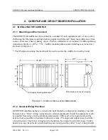
Page 13: ... be used to isolate the cardfile from earth ground 19 25 3 3 3 11 5 12 19 9 5 Fiberglass Mounting Brackets PCB Interface Connector Housing FIGURE 2 1 CARDFILE INSTALLATION DIMENSIONS 2 1 2 General Wiring Practices GENISYS II installations that are wired in the field should be configured to minimize cross talk between wires Dirty wiring connections to external equipment should be separated as much ...

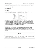
Page 14: ...cally current draw ranges from 0 1 to 7 AMPS A constant voltage type charger is recommended for the battery Note that the battery must be capable of providing a minimum voltage of 9 0 Vdc at system start up This means that anytime the OFF ON switch is operated battery voltage must be at least 9 0 V or the unit will not start 2 1 3 2 Wiring and Surge Protection Input power wiring to the GENISYS II ...

Page 15: ... 40 mm line to line and line to ground MOVs as follows a If the feed is 110 Vac use a Siemens B40K130 or a GE V131DA40 J582324 b If an isolation transformer is used also install a block type MOV on the transformer secondary line to line 4 Secondary surge suppression US S USSP units and common mode filtering are not required on the battery wiring to the cardfile 5 Connect FILTER_COM pin E32 to rack...

Page 16: ...WER INPUT WIRING AND PROTECTION To cardfile power supply PCB or external power supply converter BATT 9 0V to 36 V Battery 0 5V P P Ripple BATT Transient Voltage Suppressor Constant Voltage Charger 110V G MOVs for use in 110V system US S J582324 G E V131DA40 or Siemens B40K130 G Prime Ground Bus G Commercial 110 Vac ...

Page 17: ...installing GENISYS II printed circuit boards and a local control panel when applicable into the cardfile A Refer to Figure 2 3 With the following exceptions any plug in PCB may be installed in any cardfile slot Slot 19 cannot be used because there is no corresponding buss connector Power supply PCB N17063001 which has a two slot wide front panel should be installed in slot 18 If the cardfile is to...

Page 18: ...replacement board for a given slot Refer to Section 2 2 2 for keying plug installation procedures FIGURE 2 3 CARDFILE PCB AND PANEL INSTALLATION GUIDELINES LCP Drivers N 1 00 2801 7 Power Supply PCB N17063001 1 __ 1 111I I I I I I I I I I I Sample Locations for LCP Non vital 1 0 PCB N17002801 and Local Control Panel N16901301 II I I I I I j I I I I I I II I I Power Supply PCB N17063001 1 2 3 _4 _5...

Page 19: ... for the board part number Prior to installing a board insert keying plugs P N J709146 0473 into the corresponding cardfile motherboard keying guide as shown in Figure 2 4 and as listed in Table 2 1 If it becomes necessary to change the type of board installed in a given slot the previously installed keying plugs can be removed using a knife or a pair of needle nose pliers 96 pin Female Connector ...

Page 20: ...each board is installed These boards are the CPU board and the power supply board 2 2 3 1 Configuring the CPU Board 2 2 3 1 1 Jumper Settings See Figure 2 5 Prior to installing the CPU board in the GENISYS II cardfile the following jumpers should be checked to make certain they are in their proper positions per the system application logic software or factory requirements NOTE BOLD FACE LETTERS IN...

Page 21: ...sition 1 2 JMP18 COM1 RX CLK 9 83Mhz Position 1 2 JMP19 Not Available N A JMP20 FLASH 3 Programming Language Application space Locked Program Position 1 2 Position 2 3 2 JMP21 FLASH 1 Programming Language Executive space Locked Program Position 1 2 Position 2 3 2 JMP22 FLASH 2 Programming Language Executive space Locked Program Position 1 2 Position 2 3 2 JMP23 FLASH 4 Programming Language Applica...

Page 22: ...formation 3 Either the maintenance port or serial port 4 can be routed to the top rear CPU connector If the maintenance port is routed to the rear connector serial port 4 is not available on the top rear CPU connector 2 2 3 1 2 DIP Switch SW1 Currently only switch 1 is used Switch 1 should be set in the OPEN position The remaining rockers should be left in the closed position 2 2 3 1 3 PCMCIA Card...

Page 23: ...during boot mode operations c J1 c J2 Ec J3 Nc J4 OPEN 57600 BAUD ___ __ CLOSED 19200 BAUD JMP25 1 2 3 4 6 SW1 1 IO O O I c JJMP 33 1 IO O O I c iJMP 32 JMP29 Bottom JMP28 Top 1 2 Lock 2 3 Program Jumpers 20 24 rnrn P O O P 2 0 0 2 8 9 JMP27 1 o o o 1 N HZ I rn rn rn rn rn rn rn rn P O P O P O P O P O P O P O P O 1 1 1 1 1 1 1 1 1 0 2 0 3 0 4 0 5 0 6 0 7 O 8 0 11 12 13 14 15 16 j 17 18 illi JMP30 ...

Page 24: ...BOARD GENTLY ROCK THE BOARD TO ENGAGE THE MALE AND FEMALE CONNECTORS IF THE BOARD STILL CANNOT BE FULLY INSERTED INTO THE CARD SLOT REMOVE THE BOARD FROM THE CARDFILE AND ATTEMPT TO DETERMINE THE SOURCE OF THE RESISTANCE 4 Gently push the board into the cardfile until the board and cardfile connectors are fully engaged If the board has an integral front panel make certain that the rear face of the...

Page 25: ...e connector housing However non vital I O PCB N17061501 may need to use both openings to accommodate the full set of 32 input and 32 output wires For some GENISYS II circuit boards the connector housing also includes an Address Select PCB with 6 two position jumpers used to set the cardfile electrical address of the associated board These addresses are defined in the GENISYS II application logic r...

Page 26: ...853 J709146 0921 Harting 09 06 000 8482 Harting 09 06 000 8481 Harting 09 06 000 8484 Crimp tool for 48 pin 16 to 20 wire 48 pin 20 to 26 wire 96 pin 20 to 28 wire Harting tool 09 99 000 0077 Harting tool 09 00 000 0076 Harting tool 09 00 000 0075 Extraction tool for 48 pin 16 to 20 wire 48 pin 20 to 26 wire 96 pin 20 to 28 wire Harting tool 09 99 000 0087 Contact US S Harting tool 09 99 000 0101 ...

Page 27: ... Connector PerView A C1 B1 A1 C32 B32 A32 Narrow 96 pin Connector For Non Vital 1 0 PCB N17061501 Only Wide 48 pin Connector perView A E1 C1 Ill Ill Ill Ill Ill Ill Ill Ill Ill Ill Ill Ill Ill Ill Ill Ill Ill Ill A1 E32 C32 A32 Wide 48 pin Connector For All Other PCBs Housing Cover 0 Housing Assembly Screws 0 0 C SW1 0 1 SW2 0 1 SW3 0 1 SW4 0 1 SW5 0 1 SW6 0 1 Address Select PCB ...

Page 28: ...lf mounting requires the use of this kit TABLE 2 4 GENISYS II PC SHELF MOUNTING KIT Fig 2 7 Item Description US S Part No Comments Vendor Part No 1 Shelf mounting kit X16903906 FIGURE 2 7 SHELF MOUNTING KIT Installation standoffs included in Shelf Mounting Kit using existing hardware from front mounting 1 0 f f 0 l ____o_ ______ l 0 ...

Page 29: ... front panel The maintenance port connections may optionally be redirected using on board jumpers to replace TXD RXD and COM for serial port 4 on the top rear connector The four general purpose ports can be used for non vital serial communications with a MICROLOK II system a MICROLOK system a MICROTRAX End of Siding system or any other GENISYS system For installations where the GENISYS II system i...

Page 30: ... 50 Hz to Power Supply C24 12 V C26 12V 2 RXD E2 E4 E6 E8 C2 C4 C6 CB C10 _ C12 A2 A4 A10 A12 A32 A16 A18 A20 A22 A24 A26 A28 A30 A6 E10 E12 E14 E16 E18 C14 A8 Jti ji REF RTS RXCLK C16 C18 C20 0 C22 A14 Comm Port 1 RS 485 TXD___l_ 9 pin COM 2 k Conn Comm Ports RS 232 to Laptop PC OR RXD ___Q2t 7 TXD _Ql t 7 COM_ c JJlf Depending on JMP32 and JMP 33 Settings CPU PCB N17061301 Comm Port2 RS 485 Comm...

Page 31: ...d Output Voltage Range Externally Available Inputs Externally Available Outputs Current Rating on Outputs N17061501 32 32 6 0 to 30 0 Vdc 32 32 Outputs 1 30 0 25A polyswitch protected Outputs 31 32 5 0A fuse Suitable for lighting lamps up to 25W All inputs are activated from a positive voltage relative to battery negative over the 6 0 Vdc to 30 0 Vdc range All outputs are delivered from a low side...

Page 32: ...Address SelectPCl 3 _ _ _ j iGNO I i E 1 lnput1 __ ___u_i 81 Input 2 1 i 1 c1 Input 3 iA2 Input 4 _Ji lnpul5 lnput6 i lnput7 Input 8 Input 9 Input 10 Input 11 Input 12 This connector continued at right Non vital Output PCB N17061501 v 1 ___L Connect Loads as Shown Above I j j i i 4 5 16 17 8 9 0 1 i 2 3 24 Connect one output common for each 2 Amps of required output 1 1 J B 17______J Input Common ...

Page 33: ...the external load at supply voltage less 2 5 volts or more All 32 outputs are polyswitch protected Figure 2 10 shows a basic interface wiring diagram for this board 2 4 4 Local Control Panel Driver External Input PCBs The local control panel driver external input PCB N17002801 provides 16 isolated external inputs and 16 internal inputs and 16 internal outputs used to drive an internal local contro...

Page 34: ...20 BA E6 BC E22 OUT 1A E2 OUT 17C A14 OUT 2A C2 OUT 18C E16 OUT 3A A2 OUT 19C C16 OUT 4A C4 OUT 20C A16 _ OUT SA A4 OUT 21C E18 OUT 6A _ C6 OUT 22C C18 OUT 7A A6 OUT 23C A18 OUT SA E8 OUT 24C C20 OUT 25C A20 OUT 26C C22 NB _ E10 OUT 27C A22 BB E12 OUT 28C E24 OUT 9B _ C8 OUT 29C C24 OUT 10B A8 OUT 30C A24 OUT 11 B C10 OUT 31C E26 OUT 12B OUT 32C C26 _ A10 OUT 13B _ _ C12 OUT 14B __ A12 _ OUT 15B E...

Page 35: ...E30 C30 1 _ 1N1 A30 E28 1 N1 C28 1N2 A28 A26 1 N2 1N1 E2 TYPICAL INPUT 1 N1 E4 WIRING 1N2 C2 1 N2 C4 1N3 A2 __ _ 1 N3 A4 _ 1N4 E6 1 N4 E8 ____ _ 1N5 C6 _____ 1 NS C8 __ 1N6 A6 IN6 A8 1N7 E12 1 N7 E14 1N8 _ C12 1 N8 C14 1N9 A12 1 N9 A14 1N10 E16 1 N10 E18 1 N11 C16 IN11 C18 1N12 A16 1 N12 A18 1N13 E22 1 N13 __ E24 1N14 C22 1 N14 C24 1N15 A22 1N15 A24 _ 1N16 E26 1 N16 C26 ...

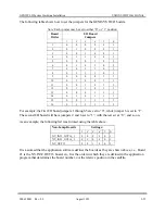
Page 36: ...w By far the best way to determine the jumper settings is to use the list file The jumper settings for each board are determined by the order in which the boards are defined in the user written application program The jumper settings do not depend on the order the boards happen to appear in the cardfile If the application program and list file are both unavailable then the order can also be found ...

Page 37: ...1 1 15 0 0 1 1 1 1 16 0 1 1 1 1 1 For example the first I O board jumpers 1 through 5 are set to 0 while jumper 6 is set to 1 The second I O board will have jumpers 2 and 6 set to 1 with the rest set at 0 and so on As an example the following list was formed using the table above Non Lamp Boards Settings 1 2 3 4 5 6 NV_IN32_OUT16_1 0 0 0 0 0 1 NV_IN32_OUT16_2 0 1 0 0 0 1 NV_OUT32 0 0 1 0 0 1 It is...

Page 38: ...UNION SWITCH SIGNAL GENISYS II System Hardware Installation 2 26 August 1999 SM 6900B Rev 0 0 ...

Page 39: ...Modems 3 4 3 2 3 Connecting to RS 485 Serial Ports Refer to Figure 3 3 3 5 3 2 4 Connecting to RS 423 Serial Ports Refer to Figure 3 4 3 6 3 2 5 Connecting to RS 232 Serial Ports 3 7 3 2 6 Isolation of Serial Port Signal Common 3 8 3 2 7 Physical Connections to Serial Ports 3 9 3 2 8 Configuring GENISYS II Serial Ports in the Application Program 3 9 3 2 9 Configuring GENISYS II CPU Serial Communic...

Page 40: ...UNION SWITCH SIGNAL GENISYS II System Hardware Installation 3 ii August 1999 SM 6900B Rev 0 0 ...

Page 41: ...l power drops the relay and closes a normally open relay contact The contact closure makes an input circuit to the non vital I O PCB in the GENISYS II cardfile see Figure 3 1 The power off relay is mounted on a plug in base and secured with a spring clip This base is designed for attachment to a standard equipment rack DIN rail or can be secured to a flat surface using a screw hole in the base und...

Page 42: ... ports The GENISYS II application program determines the function of each of these ports Each port may be designated as a GENISYS protocol master or a GENISYS protocol slave The function of serial ports may be designated in any combination The four serial ports support three different hardware interface standards Ports 1 and 2 support an RS 485 hardware interface while port 3 supports an RS 423 in...

Page 43: ... RS 423 port may be used in simple short distance multi drop applications while the RS 232 port may be used only in short distance less than 50 feet point to point applications The RS 423 port is normally reserved for direct connections to other RS 423 devices such as MICROTRAX EOS when required The RS 232 port is normally reserved for use as a GENISYS protocol slave port to be employed as a seria...

Page 44: ...r it is necessary to connect GENISYS protocol ports that are not located in the same equipment facility some type of modem or communication device that provides serial common isolation and secondary transient protection MUST be used While the operating characteristics of modems vary widely there are a few requirements that apply to all serial interface applications that employ modems GENISYS proto...

Page 45: ...nd slave ends of the communication circuit When it is available the CTS signal can be used to shorten the required delay between the assertion of RTS and the transmission of the first byte of outbound data This delay is often called the key on delay Typically when data is to be transmitted via a modem and keying of carrier is required RTS is asserted and a delay timer is started by the serial port...

Page 46: ... resistor for the master DCD input should be 240 ohms watt rather than 120 ohms to maintain the required circuit impedance for the biased circuit If the CTS input on any serial port is available but not used it should be forced to its unasserted state To permanently force an unused RS 485 input to its unasserted state the input should be connected to 5V and the input should be connected to COMMON ...

Page 47: ...nd RTS output signals and RXD and DCD input signals Each RS 232 signal is transported by a single wire and is referenced to signal common COM When any RS 232 signal is not asserted the voltage level for that signal is between 3 and 15 volts For data lines TXD and RXD the quiescent or unasserted state is the MARK state The asserted state for all signals is between 3 and 15 volts RS 232 ports should...

Page 48: ...to ground loops and to damage due to electrical surges This effectively means that devices like these must be connected to GENISYS II through a serial line isolator which provides a high level of isolation between the signal commons of GENISYS II and serial devices such as modems and data radios Isolation between serial signal commons is also necessary when serially connecting GENISYS II units to ...

Page 49: ...Serial Port Configuration for Operation on a Direct Wire Point to Point Communication Circuit GENISYS II serial ports 1 2 and 3 are designed to operate on a direct wire multi drop communication circuit When any of these three ports is designated as a GENISYS protocol slave port the default port configuration is set by the GENISYS II compiler to accommodate a multi drop communication circuit This c...

Page 50: ...ion information that accompanies the modem When simple frequency shift modems are used such as those manufactured by RFL Industries 8 to 12 bit times is a good value for key on and key off delays More sophisticated modems and more sophisticated communication links those with regenerative repeaters for example may require longer key on and key off delays The approximate required key on and key off ...

Page 51: ...nit that is heavily loaded many complex logic equations in the application program that execute very frequently The polling interval is the time inserted between the completion of one message exchange initiated by the master port and the start of the next Typically the default value for this parameter should be used Increasing the value of this parameter decreases the load on the GENISYS II proces...

Page 52: ...n JUMPER FUNCTION POSITION EFFECT JMP7 Port 4 receive data input 1 2 2 3 ENABLED DISABLED JMP8 Port 4 data carrier detect input 1 2 2 3 ENABLED DISABLED JMP10 Port 1 synchronous transmitter clock 1 2 2 3 INPUT OUTPUT JMP11 Port 3 output driver low level 1 2 2 3 RS 232 RS 423 JMP12 Port 3 output driver high level 1 2 2 3 RS 232 RS 423 JMP13 Port 3 synchronous transmitter clock 1 2 2 3 INPUT OUTPUT ...

Page 53: ...5 Vdc regulated power source that may be provided by the connected GENISYS II unit and a 12 Vdc battery power source that drives the 20 mA current loops Faston terminals are provided on the panel for power connections 3 3 2 Interface Wiring FIGURE 3 2 shows a typical 20 mA current loop interface between master and slave GENISYS II systems using the serial communications adapter panel Transmit Data...

Page 54: ...DCDCOM 11 TXD IN 22 RXD OUT RTS OUT 24 SIG COM RTSCOM TXD OUT 10 TXD COM 12 Serial Communications Adapter Panel Equipment House Case Current Loop Cable Twisted Pair Wires l V V J2 10 TXD OUT 12 TXD COM 22 RTS OUT 24 RTS COM 9 DCD IN 11 DCD COM 21 RXD IN 23 RXD COM 37 pin Connector l J1 5 RTS IN N 13 N DCD OUT 14 TXD IN N 16 RXD OUT 1 SIGGND N Serial Communications Adapter Panel Equipment House Cas...

Page 55: ...ield wire at the end of the cable should be grounded using one of the 25 pin D connector attachment screws on the interface panel In addition a rack ground wire should be run from the panel s EARTH GROUND dual Fasten terminal to the equipment rack prime ground bus Keep this wire as short as possible and minimize the number of bends The current loop cable should also be provided strain relief by se...

Page 56: ...lave on the circuit only Load resistor Lm is 240 ohm watt and is installed on master DCD only as shown 5 Do not connect serial port common to ground FIGURE 3 3 TYPICAL GENISYS II MASTER TO GENISYS II SLAVE RS 485 DIRECT WIRE SERIAL INTERFACE UNITS POWERED BY SAME BATTERY HALF DUPLEX GENISYS PROTOCOL MASTER SLAVE GENISYS II CONNECTION GENISYS II CPU CONN A TO ADDITIONAL CPU CONN A SLAVES PORT2 PORT...

Page 57: ...2 CTS E18 RXREF C18 COM R DCD E10 RXD E14 TXD E16 RTS C14 12V C26 CTS E12 COM C18 RXCOM E18 1 Resistor R is 10K ohm watt 2 For full duplex GENISYS protocol connection RTS and DCD need not be connected 3 Serial commons are interconnected through battery that powers units FIGURE 3 4 TYPICAL GENISYS II MASTER TO GENISYS II SLAVE RS 423 DIRECT WIRE SERIAL INTERFACE UNITS POWERED BY SAME BATTERY HALF D...

Page 58: ...ERIAL ISOLATOR GENISYS PROTOCOL MASTER OR SLAVE GENISYS II TO GENISYS II BATTERY CPU CONN A N12 B12 RFL CARRIER SET PORT4 RTS A14 24 24 REQUEST TO SEND OR KEY ON C20 TXD 25 25 DATA OUT C22 RXD 12 12 DATA IN DCD C16 23 23 DATA CARRIER DETECT OR SQUELCH E22 COM 10 10 SIGNAL COMMON _ SERIAL COMMUNICATION CIRCUIT ISOLATION UNIT N16401101 MASTER OR SLAVE GENISYS II TO GENISYS II BATTERY CPU CONN A N12 ...

Page 59: ... 7 TYPICAL GENISYS 2000 MASTER TO GENISYS II SLAVE RS 232 DIRECT WIRE SERIAL INTERFACE UNITS POWERED BY SAME BATTERY GENISYS PROTOCOL GENISYS CPU CONN A GENISYS II CPU CONN A MASTER PORT PORT 4 DCD RXD TXD RTS COM 2 1 4 5 J 7 U MRTS MTXD MRXD MDCD MCOM MDSR 12V MCTS C16 C22 C20 A14 E22 6 FIGURE 3 8 TYPICAL GENISYS MASTER TO GENISYS II SLAVE RS 232 DIRECT WIRE SERIAL INTERFACE UNITS POWERED BY SAME...

Page 60: ...UNION SWITCH SIGNAL GENISYS II System Hardware Installation 3 20 August 1999 SM 6900B Rev 0 0 ...

Page 61: ... 4 1 4 1 MAJOR SYSTEM ASSEMBLIES 4 1 4 2 MAJOR CARDFILE COMPONENTS 4 1 4 2 1 Plug in Printed Circuit Boards and Front Panels 4 1 4 2 2 PCB Interface Cable Assembly Components and Tools 4 2 4 2 3 Misc Cardfile Installation Parts 4 2 4 3 POWER SIGNAL CONDITIONING AND PROTECTION EQUIPMENT 4 3 4 4 MISCELLANEOUS UNIT INSTALLATION HARDWARE 4 3 ...

Page 62: ...UNION SWITCH SIGNAL GENISYS II System Hardware Installation 4 ii August 1999 SM 6900B Rev 0 0 ...

Page 63: ...ial Communications Adapter Panel N451460 3001 Reference Section 4 4 for installation hardware 4 2 MAJOR CARDFILE COMPONENTS 4 2 1 Plug in Printed Circuit Boards and Front Panels Item Description US S Part No Comments CPU PCB N17061310 Power Supply PCB N17063001 Non Vital I O PCB N17061501 32 inputs 32 outputs non isolated Non Vital Output PCB N17062701 32 isolated outputs Input LCP Driver PCB N170...

Page 64: ...pin housing Replaces N17002002 N17003301 96 pin housing Replaces N17002101 EEPROM PCB N17002001 CPU PCB connector assembly only Crimp Tools 48 pin 16 20 Harting 09 99 000 0077 48 pin 20 26 Harting 09 00 000 0076 96 pin 20 28 Harting 09 00 000 0075 Extraction Tools 48 pin 16 20 Harting 09 99 000 0087 Contact US S 48 pin 20 26 Wire 96 pin 20 28 Harting 09 99 000 0101 Insertion Tools Contact US S 48 ...

Page 65: ...2 2 Equivalent GE V131DA40 or Siemens B40K130 Transient Voltage Suppressor J792736 0032 Application Cardfile system power input Reference Section 2 1 3 2 and Figure 2 2 Equivalent 5KP36A 4 4 MISCELLANEOUS UNIT INSTALLATION HARDWARE Item Description US S Part No Comments Power Off Relay Reference Section 3 1 Relay J726153 0283 Base J581782 0026 Spring Clip J680167 0009 Serial Communication Adapter ...

Page 66: ...UNION SWITCH SIGNAL GENISYS II System Hardware Installation 4 4 August 1999 SM 6900B Rev 0 0 ...

Page 67: ......

Reviews: