
SARA-G450 - System integration manual
UBX-18046432 - R08
Design-in
Page 84 of 143
C1-Public
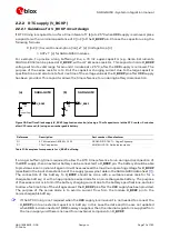
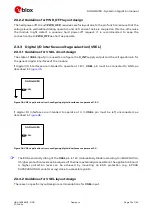
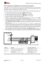
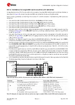
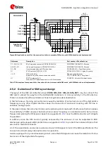
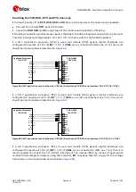
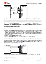
2.4.2.2
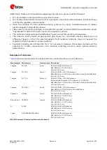
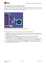
Guidelines for ANT_DET layout design
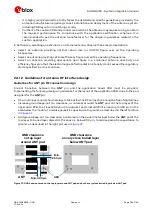
describes the recommended layout for the antenna detection circuit to be provided on the
application board to achieve antenna detection functionality, implementing the recommended
schematic described in the previous
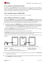
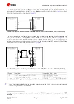
SARA module
C2
R1
D1
C1
L1
J1
C3 L2
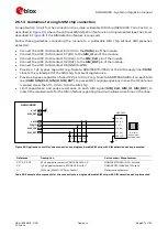
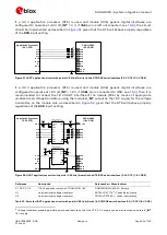
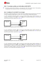
Figure 42: Suggested layout for antenna detection circuit on application board
The antenna detection circuit layout suggested in
is explained below:
The ANT pin is connected to the antenna connector by means of a 50
transmission line,
implementing the design guidelines described in section
and the recommendations of the
SMA connector manufacturer.
DC blocking capacitor at the ANT pin (C2) is placed in series to the 50
transmission line.
The ANT_DET pin is connected to the 50
transmission line by means of a sense line.
Choke inductor in series at the ANT_DET pin (L1) is placed so that one pad is on the 50
transmission line and the other pad represents the start of the sense line to the ANT_DET pin.
The additional components (R1, C1 and D1) on the ANT_DET line are placed as ESD protection.
The additional high pass filter (C3 and L2) on the ANT line are placed as ESD immunity
improvement (not strictly required).


