background image

SARA-G450 - System integration manual 

UBX-18046432 - R08 

System description 

Page 40 of 143 

C1-Public 


1.9.2


Secondary auxiliary serial interface (AUX UART) 


Secondary auxiliary UART interface is not supported by the “00” product version. This interface 
should be left unconnected and should not be driven by external devices. 


The  secondary  auxiliary  UART  interface  (AUX  UART)  is  a  3-wire  unbalanced  asynchronous  serial 
interface available over RXD_AUX (data output pin) and TXD_AUX (data input pin), supporting: 


AT command mode

11


Data mode and online command mode

11


GNSS tunneling 

SARA-G450 modules’ auxiliary UART interface is configured by default for AT commands. 

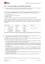
The  serial  interface  configuration  can  be  changed  by  means  of  the  +USIO  AT  command  to  select 
different  alternative  serial  interface  configuration  variants,  summarized  in 

Table  10

,  available  in  a 

mutually  exclusive  way  (for  more  details,  see  the  u-blox  AT  commands  manual 

[11]

,  +USIO  AT 

command). 


AT+USIO  UART 

AUX UART 

FT UART 

Remarks 

AT, data and MUX 

AT, data 

Diagnostic 


AT, data and MUX 

AT, data 

Diagnostic 

Default configuration 

AT, data and MUX 

AT, data 

Diagnostic 


AT, data and MUX 

GNSS tunneling 

Diagnostic 


AT, data and MUX 

GNSS tunneling 

Diagnostic 


Table 10: Alternative serial interface configuration variants supported by SARA-G4 modules product versions “01” onwards 


The  serial  interface  configuration  cannot  be  changed  on  the  “00”  product  version  of  the  
SARA-G450 modules: the +USIO AT command is not supported. 

SARA-G450 modules’ auxiliary UART interface can be configured in AT command mode by means of 
the AT+USIO command (for more details, see 

Table 10

) so that: 


the cellular module waits for AT command instructions and interprets all the characters received 
over the auxiliary UART interface as commands to be executed 


the  auxiliary  UART  interface  provides  RS-232  functionality  conforming  to  ITU-T  V.24 
recommendatio

[19]

 with CMOS compatible signal levels: 0 V for low data bit or ON state and 

1.8 V / 3 V for high data bit or OFF state (for detailed electrical characteristics, see the SARA-G450 
data sheet 

[1])


the  cellular  module  is  designed  to  operate  as  a  modem,  which  represents  the  Data 
Circuit-terminating  Equipment  (DCE)  according  to  ITU-T  V.24  recommendation 

[19]

:  the 

application processor connected to the module through the auxiliary UART interface represents 
the Data Terminal Equipment (DTE) 


Flow control is not supported 


2400, 4800, 9600, 19200, 38400, 57600 and 115200 bit/s baud rates can be set (see the u-blox AT 
commands manual 

[11]

, +IPR) 


8N1, 8E1, 8O1 or 8N2 frame format can be set (see the u-blox AT commands manua

[11]

, +ICF) 


11

 See the u-blox AT commands manua

[11]

 for the definition of the command mode, data mode, and online command mode. 

Summary of Contents for SARA-G450 Series

Page 1: ...ystem integration manual Abstract This document describes the features and the system integration of the SARA G450 quad band GSM GPRS cellular modules These modules are a complete and cost efficient solution offering voice and or data communication in the compact SARA form factor ...

Page 2: ...cument contains the final product specification This document applies to the following products Product name Type number Modem version Application version PCN reference Product status SARA G450 SARA G450 00C 00 09 02 A02 01 UBX 18067098 End of life SARA G450 00C 01 09 02 A03 17 UBX 20033037 Mass production SARA G450 01C 00 09 02 A04 23 UBX 20033037 Initial production u blox or third parties may ho...

Page 3: ...na interface 27 1 7 1 Antenna RF interface ANT 27 1 7 2 Antenna detection interface ANT_DET 28 1 8 SIM interface 28 1 8 1 U SIM card interface 28 1 8 2 SIM card detection interface SIM_DET 28 1 9 Serial interfaces 29 1 9 1 Primary main serial interface UART 29 1 9 2 Secondary auxiliary serial interface AUX UART 40 1 9 3 Additional serial interface for FW upgrade and tracing FT UART 42 1 9 4 DDC I2...

Page 4: ...5 2 4 2 Antenna detection interface ANT_DET 82 2 5 SIM interface 85 2 5 1 Guidelines for SIM circuit design 85 2 5 2 Guidelines for SIM layout design 90 2 6 Serial interfaces 91 2 6 1 Primary main serial interface UART 91 2 6 2 Secondary auxiliary serial interface AUX UART 98 2 6 3 Additional serial interface for FW upgrade and Tracing FT UART 99 2 6 4 DDC I2C interface 100 2 7 Audio interfaces 10...

Page 5: ...es 122 4 Approvals 123 4 1 Product certification approval overview 123 4 2 European conformance 124 4 3 Chinese compulsory certification 124 5 Product testing 125 5 1 u blox in series production test 125 5 2 Test parameters for OEM manufacturer 125 5 2 1 Go No go tests for integrated devices 126 5 2 2 Functional tests providing RF operation 126 Appendix 127 A Migration between SARA modules 127 A 1...

Page 6: ...th a comprehensive feature set including an extensive set of internet protocols The modules are also designed to provide fully integrated access to u blox GNSS positioning chips and modules with embedded A GPS AssistNow Online and AssistNow Offline functionality Any host processor connected to the cellular module through a single serial port can control both the cellular module and the positioning...

Page 7: ...lable interfaces V_BCKP RTC V_INT I O 26 MHz 32 768 kHz RF transceiver Power Management Unit Baseband ANT Switch PA VCC supply Memory Power off Power on SIM card SIM card detection UART primary main UART secondary auxiliary DDC I2C Analog audio MIC SPK GPIOs Antenna detection VSEL I O voltage selection UART flashing tracing 32 768 kHz over GPIO Figure 1 SARA G450 modules block diagram 1 Device can...

Page 8: ...h 26 MHz crystal connected to the digital controlled crystal oscillator to perform the clock reference in active mode and connected mode The Baseband and Power Management section is composed of the following main elements Baseband processor Memory system Voltage regulators to derive all the system supply voltages from the module supply VCC Circuit for the RTC clock reference in low power idle mode...

Page 9: ...ical if VSEL is connected to GND V_INT 3 V typical if VSEL is unconnected Test Point recommended for diagnostic purpose See section 1 5 3 for functional description See section 2 2 3 for external circuit design in System PWR_ON 15 I Power on input Internal 28 k active pull up to 2 5 V internal supply Test Point recommended for diagnostic purpose See section 1 6 1 for functional description See sec...

Page 10: ...2 I UART data input Circuit 103 TxD in ITU T V 24 for AT command data Mux and FOAT It operates at V_INT voltage level See section 1 9 1 for functional description See section 2 6 1 for external circuit design in CTS 11 O UART clear to send output Circuit 106 CTS in ITU T V 24 It operates at V_INT voltage level See section 1 9 1 for functional description See section 2 6 1 for external circuit desi...

Page 11: ...or diagnostic purpose See section 1 9 3 for functional description See section 2 6 3 for external circuit design in DDC SCL 27 O I2C bus clock line Fixed open drain for communication with u blox positioning modules chips It operates at V_INT voltage level External pull up required See section 1 9 4 for functional description See section 2 6 4 for external circuit design in SDA 26 I O I2C bus data ...

Page 12: ...ceive data Not supported I2S_TXD 35 O I2S transmit data Not supported I2S_WA 34 O I2S word alignment Not supported GPIO GPIO1 16 I O GPIO It operates at V_INT voltage level See sections 1 11 for functional description See sections 2 8 for external circuit design in GPIO2 23 I O GPIO It operates at V_INT voltage level See sections 1 11 for functional description See sections 2 8 for external circui...

Page 13: ...s internally generated When valid VCC supply is applied the module switches from not powered mode to power off mode see section 1 5 1 When the module is switched off by an appropriate power off event or by a PWR_OFF abrupt shutdown the module enters power off mode see section 1 6 2 When in power off mode the module can be switched on by PWR_ON or RTC alarm the module switches from power off mode t...

Page 14: ...mode When a voice call or a data transmission is terminated the module returns to active mode Connected A voice call or a data transmission is in progress The module is ready to communicate with an external device by means of the application interfaces When a voice call or a data transmission is initiated the module enters connected mode from active mode When a voice call or a data transmission is...

Page 15: ...ximum power level in connected mode as described in section 1 5 1 2 to the low current consumption during low power idle mode with power saving enabled as described in section 1 5 1 3 SARA G450 modules provide separate supply inputs over the three VCC pins VCC pins 52 and 53 represent the supply input for the internal RF power amplifier demanding most of the total current drawn of the module when ...

Page 16: ... current Support with adequate margin the highest averaged VCC current consumption value in connected mode conditions specified in the SARA G450 data sheet 1 The highest averaged VCC current consumption can be greater than the specified value according to the actual antenna mismatching temperature and VCC voltage See section 1 5 1 2 for 2G connected mode current profiles VCC peak current Support w...

Page 17: ... in the low bands due to the 3GPP transmitter output power specifications During a GSM transmission current consumption is not so significantly high in receiving or in monitor bursts and it is low in the bursts unused to transmit receive Figure 4 shows an example of the module current consumption profile versus time in GSM talk mode Time ms RX slot unused slot unused slot TX slot unused slot unuse...

Page 18: ...gure 6 illustrates the current consumption profiles in GPRS connected mode in the 850 or 900 MHz bands with 2 slots used to transmit and 1 slot used to receive as for the GPRS multi slot class 10 Time ms RX slot unused slot unused slot TX slot TX slot unused slot MON slot unused slot RX slot unused slot unused slot TX slot TX slot unused slot MON slot unused slot GSM frame 4 615 ms 1 frame 8 slots...

Page 19: ... its reference clock frequency from 32 kHz to the 26 MHz used in active mode The time period between two paging block receptions is defined by the network This is the paging period parameter fixed by the base station through broadcast channel sent to all users on the same serving cell For 2G radio access technology the paging period varies from 470 8 ms DRX 2 length of 2 x 51 2G frames 2 x 51 x 4 ...

Page 20: ...nt consumption profile of the SARA G450 modules when power saving is disabled the module is registered with the network active mode is maintained and the receiver and the DSP are periodically activated to monitor the paging channel for paging block reception ACTIVE MODE 0 47 2 12 s Paging period Time s Current mA 100 50 0 Time ms Current mA 100 50 0 RX Enabled DSP Enabled Figure 9 VCC current cons...

Page 21: ...e specified in the Input characteristics of Supply Power pins table in the SARA G450 data sheet 1 See the u blox AT commands manual 11 for more details The RTC can be supplied from an external back up battery through the V_BCKP when the main voltage supply is not provided to the module through VCC This lets the time reference date and time run until the V_BCKP voltage is within its valid range eve...

Page 22: ...he module is switched on V_INT can be configured in the two following ways V_INT 1 8 V if VSEL pin is connected to GND V_INT 3 V if VSEL pin is left unconnected 1 6 System function interfaces 1 6 1 Module power on PWR_ON 1 6 1 1 Switch on events When the SARA G450 modules are in the not powered mode i e switched off with the VCC module supply not applied valid VCC supply must be applied first swit...

Page 23: ...n a correct sequence from the reset state to the default operational state The module is fully ready to operate after all the interfaces are configured VCC V_BCKP PWR_ON PWR_OFF V_INT Internal reset System state Digital pins state Internal reset Operational Tristate Floating OFF ON Internal reset Operational 0 ms 35 ms 3 s Start of interface configuration Module interfaces are configured Start up ...

Page 24: ...on volatile memory and a clean network detach is not performed It is highly recommended to avoid an abrupt hardware shutdown of the module by forcing a low level on PWR_OFF input pin during module normal operation the PWR_OFF line should be set low only if reset or shutdown via AT commands fails or if the module does not reply to a specific AT command after a time period longer than the one define...

Page 25: ...n power off mode as long as a switch on event does not occur e g applying an appropriate low level to the PWR_ON input and enters not powered mode if the supply is removed from the VCC pins VCC V_BCKP PWR_ON PWR_OFF V_INT Internal reset System state Digital pins state Operational OFF Tristate Floating ON Operational Tristate AT CPWROFF sent to the module 0 s 2 5 s 5 s OK replied by the module VCC ...

Page 26: ...ds fails or if the module does not reply to a specific AT command after a time period longer than the one defined in the u blox AT commands manual 11 The PWR_OFF input pin is internally connected through a series Schottky diode to 1 5 V internal supply keeping the line to the high logic level when the PWR_OFF pin is not forced low from the external See the SARA G450 data sheet 1 for the detailed e...

Page 27: ...RF termination must match as much as possible the 50 impedance of the ANT pin over the operating frequency range reducing as much as possible the amount of reflected power Efficiency 1 5 dB 70 recommended 3 0 dB 50 acceptable The radiation efficiency is the ratio of the radiated power to the power delivered to antenna input the efficiency is a measure of how well an antenna receives or transmits T...

Page 28: ...ion and configuration of the voltage required by the connected U SIM card or chip Both 1 8 V and 3 V SIM types are supported activation and deactivation with automatic voltage switching from 1 8 V to 3 V is implemented according to ISO IEC 7816 3 specifications The VSIM supply output pin provides internal short circuit protection to limit start up current and protect the device in short circuit si...

Page 29: ...by external devices DDC I2C interface is not supported by the 00 product version This interface should be left unconnected and should not be driven by external devices 1 9 1 Primary main serial interface UART 1 9 1 1 UART features The UART interface is a 9 wire unbalanced asynchronous serial interface supporting AT command mode4 Data mode and Online command mode4 Multiplexer protocol functionality...

Page 30: ...odule data line input HW flow control handshakes or none flow control are supported by the UART interface and can be set by AT commands see u blox AT commands manual 11 K IFC AT commands Hardware flow control is enabled by default SARA G450 modules support one shot autobauding the baud rate automatic detection is performed once at module start up at first AT command received After detection the mo...

Page 31: ...e command mode8 and issues an OK result code AT C1 Circuit 109 changes in accordance with the Carrier detect status ON if the Carrier is detected OFF otherwise MUX protocol disabled Multiplexing mode is disabled by default and it can be enabled by AT CMUX command Table 8 Default UART AT interface configuration 1 9 1 3 UART signal behavior At the module switch on before the UART interface initializ...

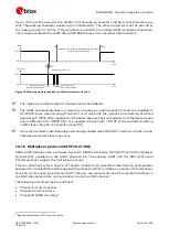
Page 32: ...s still used as a power state indicator The CTS hardware flow control setting can be changed by AT commands for more details see the u blox AT commands manual 11 AT K AT IFC AT UCTS commands description If the hardware flow control is not enabled after the UART initialization the CTS line behaves as per AT UCTS command setting When the power saving configuration is enabled and the hardware flow co...

Page 33: ...FF state if the line is not activated by the DTE an active pull up is enabled inside the module on the DTR input Module behavior according to DTR status can be changed by AT command for more details see the u blox AT commands manual 11 AT D command description DCD signal behavior If AT C1 is set as it is by default the DCD module output line is set by default to the OFF state high level at UART in...

Page 34: ...lization During an incoming call the RI line is switched from the OFF state to the ON state with a 4 1 duty cycle and a 5 s period ON for 1 s OFF for 4 s see Figure 15 until the DTE attached to the module sends the ATA string and the module accepts the incoming call The RING string sent by the module DCE to the serial port at constant time intervals is not correlated with the switch of the RI line...

Page 35: ...abled the module automatically enters low power idle mode whenever possible and otherwise the active mode is maintained by the module see section 1 4 for definition and description of module operating modes referred to in this section The AT UPSV command configures both the module power saving and also the UART behavior in relation to the power saving The conditions for the module entering idle mo...

Page 36: ...r OFF The first character sent by the DTE is lost but after 20 ms the UART and the module are woken up recognition of subsequent characters is guaranteed after the complete UART module wake up Data sent by the module is correctly received by the DTE if it is ready to receive data otherwise data is lost 2 Enabled AT K3 ON or OFF Not Applicable HW flow control cannot be enabled with AT UPSV 2 2 Disa...

Page 37: ... 11 ms The time period from the last data received at the serial port during the active mode the module does not enter idle mode until a timeout expires The second parameter of the UPSV AT command configures this timeout from 40 2G frames i e 40 x 4 615 ms 185 ms up to 65000 2G frames i e 65000 x 4 615 ms 300 s Default value is 2000 2G frames i e 2000 x 4 615 ms 9 2 s The active mode duration can ...

Page 38: ...from the low power idle mode to active mode within 20 ms from the first character received this is the system wake up time As a consequence the first character sent by the DTE when the UART is disabled i e the wake up character is not a valid communication character even if the wake up via data reception configuration is active because it cannot be recognized and the recognition of the subsequent ...

Page 39: ...g at a fixed baud rate of 115200 bit s regardless of the baud rate previously recognized So if the desired baud rate is different from 115200 bit s it is needed to be set with IPR AT command before setting UPSV see u blox AT commands manual 11 It is recommended to avoid having power saving enabled when the UART interface is in data mode otherwise some data loss may occur 1 9 1 5 Multiplexer protoc...

Page 40: ...uration variants supported by SARA G4 modules product versions 01 onwards The serial interface configuration cannot be changed on the 00 product version of the SARA G450 modules the USIO AT command is not supported SARA G450 modules auxiliary UART interface can be configured in AT command mode by means of the AT USIO command for more details see Table 10 so that the cellular module waits for AT co...

Page 41: ...AT commands data communication and multiplexer functionalities while the secondary auxiliary UART can be used for AT commands and data communication See the Multiple AT command interfaces appendix in the u blox AT commands manual 11 for further details regarding multiple AT command interfaces general usage and related AT command profile configurations The power saving configuration is controlled b...

Page 42: ... the VSEL input pin setting 1 9 4 DDC I2C interface DDC I2C interface is not supported by the 00 product version This interface should be left unconnected and should not be driven by external devices SARA G450 modules provide an I2C compatible DDC interface on the SCL and SDA pins exclusively for the communication with u blox GNSS positioning chips modules The AT command interface is not available...

Page 43: ...ioning receiver power consumption When the GNSS functionality is not required the positioning receiver can be completely switched off by the cellular module that is controlled by AT commands For more details regarding the handling of the DDC I2C interface the GNSS aiding features and the GNSS related function over GPIOs see section 1 11 the u blox AT commands manual 11 UGPS UGPRF UGPIOC AT command...

Page 44: ...ound line for the external microphone circuit Analog audio output o Differential audio output SPK_P SPK_N shared for all the analog audio path modes the pins can be connected to the input of an external analog audio device or can be connected to an external speaker 1 10 1 Analog audio interface Analog audio interface is not supported by the 00 product version This interface should be left unconnec...

Page 45: ...ble disable the supply of an external u blox GNSS receiver connected to the cellular module by the DDC I2C interface GPIO212 GPIO112 GPIO212 GPIO312 GPIO412 Last gasp12 Input to trigger last gasp notification GPIO112 GPIO212 GPIO312 GPIO412 32 768 kHz output 32 768 kHz clock output GPIO3 General purpose input Input to sense high or low digital level GPIO1 GPIO2 GPIO3 GPIO4 General purpose output O...

Page 46: ...t of coverage conditions limited service conditions when roaming to networks not supporting the specific SIM limited service in cells which are not suitable or barred due to operators choices no cell condition when moving to poorly served or highly interfered areas In the latter case interference can be artificially injected in the environment by a noise generator covering a given spectrum thus ob...

Page 47: ...13 6 HTTP SARA G450 modules support Hyper Text Transfer Protocol HTTP 1 0 functionalities as an HTTP client is implemented HEAD GET POST DELETE and PUT operations are available The file size to be uploaded downloaded depends on the free space available in the local file system FFS at the moment of the operation Up to 4 HTTP client contexts can be used simultaneously SARA G450 modules support also ...

Page 48: ...full power In this case its temperature can increase very quickly and can raise the temperature nearby The best solution is always to properly design the system where the module is integrated Nevertheless having an extra check security mechanism embedded into the module is a good solution to prevent operation of the device outside of the specified range Smart temperature supervisor STS The smart t...

Page 49: ...ation interface who can take if possible the necessary actions to return to a safer temperature range or simply ignore the indication The module is still in a valid and good working condition Outside the valid temperature range Ti t 2 or Ti t 2 the device is working outside the specified range and represents a dangerous working condition This condition is indicated and the device shuts down to avo...

Page 50: ...ress Shut the device down Yes No Yes Yes No No No Yes Send shutdown notification Feature enabled full logic or indication only IF Full Logic Enabled Feature disabled no action Temperature is within normal operating range Yes Tempetature is within warning area Tempetature is outside valid temperature range No Feature enabled in full logic mode Feature enabled in indication only mode no further acti...

Page 51: ...13 10 AssistNow clients and GNSS integration Not supported by the 00 product version For customers using u blox GNSS receivers the SARA G450 modules feature embedded AssistNow clients AssistNow A GPS provides better GNSS performance and faster Time To First Fix The clients can be enabled and disabled with an AT command see the u blox AT commands manual 11 SARA G450 modules act as a stand alone Ass...

Page 52: ...tabase SARA G450 modules can either send the parameters of the visible home network cells only normal scan or the parameters of all surrounding cells of all mobile operators deep scan The CellLocate database is compiled from the position of devices which observed in the past a specific cell or set of cells historical observations as follows 1 Several devices reported their position to the CellLoca...

Page 53: ...s implemented through a set of three AT commands that allow GNSS receiver configuration ULOCGNSS CellLocate service configuration ULOCCELL and requesting the position according to the user configuration ULOC The answer is provided in the form of an unsolicited AT command including latitude longitude and estimated accuracy if the position has been estimated by CellLocate and additional parameters i...

Page 54: ...processor must proceed in the following way Send the UFWUPD AT command through the AT interface specifying file type and desired baud rate Reconfigure serial communication at selected baud rate with the used protocol Send the new FW image via the used protocol After FW image is sent module reboots and can stay unresponsive up to 2 minutes with V_INT low it is strongly recommended not to remove VCC...

Page 55: ...an be woken up from idle mode to active mode by the connected application processor or by network activities as described in Table 5 During idle mode the module processor core runs with the RTC 32 kHz reference clock which is generated by an internal oscillator For the complete description of the UPSV AT command see the u blox AT commands manual 11 For the definition and the description of SARA G4...

Page 56: ...ON PWR_OFF VSEL pins Accurate design is required to guarantee that the voltage level is well defined during operation Carefully follow the suggestions provided in section 2 3 for schematic and layout design 5 Analog audio interface MIC_BIAS MIC_GND MIC_P MIC_N uplink and SPK_P SPK_N downlink pins Accurate design is required to obtain clear and high quality audio reducing the risk of noise from aud...

Page 57: ...e use of switching step down provides the best power efficiency for the overall application and minimizes current drawn from the main supply source See sections 2 2 1 2 2 2 1 6 2 2 1 10 and 2 2 1 11 for specific design in The use of an LDO linear regulator becomes convenient for a primary supply with a relatively low voltage e g less than 5 V In this case the typical 90 efficiency of the switching...

Page 58: ... recommended However if the selected regulator or battery is not able to support the highest peak current of the module it must be able to support at least the highest averaged current consumption value specified in the SARA G450 data sheet 1 The additional energy required by the module during a 2G Tx slot can be provided by an appropriate bypass tank capacitor or supercapacitor with very large ca...

Page 59: ...YNC BD BOOST SW FB GND 6 7 10 9 5 C6 1 2 3 8 11 4 C7 C8 D1 R4 R5 L1 C3 U1 52 VCC 53 VCC 51 VCC GND Figure 23 Suggested schematic design for the VCC voltage supply application circuit using a step down regulator Reference Description Part number Manufacturer C1 10 µF capacitor ceramic X7R 5750 15 50 V C5750X7R1H106MB TDK C2 10 nF capacitor ceramic X7R 0402 10 16 V GRM155R71C103KA01 Murata C3 680 pF...

Page 60: ...a C2 100 µF capacitor tantalum B_SIZE 20 6 3V 15m T520B107M006ATE015 Kemet C3 5 6 nF capacitor ceramic X7R 0402 10 50 V GRM155R71H562KA88 Murata C4 6 8 nF capacitor ceramic X7R 0402 10 50 V GRM155R71H682KA88 Murata C5 56 pF capacitor ceramic C0G 0402 5 50 V GRM1555C1H560JA01 Murata C6 220 nF capacitor ceramic X7R 0603 10 25 V GRM188R71E224KA88 Murata D1 Schottky diode 25V 2 A STPS2L25 STMicroelect...

Page 61: ...in Table 15 show an example of a high reliability power supply circuit where the VCC module supply is provided by an LDO linear regulator capable of delivering the specified highest peak pulse current with an appropriate power handling capability The regulator described in this example supports a wide input voltage range and it includes internal circuitry for reverse battery protection current lim...

Page 62: ...ramic X5R 0603 20 6 3 V GRM188R60J106ME47 Murata R1 27 k resistor 0402 5 0 1 W RC0402JR 0727KL Yageo Phycomp R2 4 7 k resistor 0402 5 0 1 W RC0402JR 074K7L Yageo Phycomp U1 LDO linear regulator ADJ 3 0 A LP38501ATJ ADJ NOPB Texas Instrument Table 16 Suggested components for low cost solution VCC voltage supply application circuit using an LDO linear regulator 2 2 1 4 Guidelines for VCC supply circ...

Page 63: ...upply the module in order to minimize series resistance losses To avoid voltage drop undershoot and overshoot at the start and end of a transmit burst during a single slot 2G transmission when current consumption on the VCC supply can rise up to the maximum peak pulse current specified in the SARA G450 data sheet 1 place a bypass capacitor with large capacitance more than 100 µF and low ESR near t...

Page 64: ...tivity rating of the VCC supply pins is 1 kV Human Body Model according to JESD22 A114 A higher protection level can be required if the line is externally accessible on the application board e g if accessible battery connector is directly connected to VCC pins A higher protection level can be achieved by mounting an ESD protection e g EPCOS CA05P4S14THSG varistor array close to the accessible poin...

Page 65: ... Application devices powered by a Li Ion or Li Polymer battery pack should implement a suitable battery charger design considering SARA G450 modules do not have an on board charging circuit In the application circuit described in Figure 29 and Table 19 a rechargeable Li Ion or Li Polymer battery pack which features suitable pulse and DC discharge current capabilities and low DC series resistance i...

Page 66: ...ta C8 56 pF capacitor ceramic C0G 0402 5 25 V GRM1555C1E560JA01 Murata C9 15 pF capacitor ceramic C0G 0402 5 25 V GRM1555C1E150JA01 Murata D1 D2 Low capacitance ESD protection CG0402MLE 18G Bourns R1 R2 24 k resistor 0402 5 0 1 W RC0402JR 0724KL Yageo Phycomp R3 3 3 k resistor 0402 5 0 1 W RC0402JR 073K3L Yageo Phycomp R4 1 0 k resistor 0402 5 0 1 W RC0402JR 071K0L Yageo Phycomp U1 Li Ion or Li Po...

Page 67: ...y source for the module and starts a charging phase accordingly The MP2617H IC normally provides a supply voltage to the module regulated from the external main primary source allowing immediate system operation even under missing or deeply discharged battery the integrated step down regulator is capable of providing up to 3 A output current with low output ripple and fixed 1 6 MHz frequency in PW...

Page 68: ... circuit Reference Description Part number Manufacturer B1 Li Ion or Li Polymer battery pack with 10 k NTC Generic manufacturer C1 C5 C6 22 µF capacitor ceramic X5R 1210 10 25 V GRM32ER61E226KE15 Murata C2 C4 C10 100 nF capacitor ceramic X7R 0402 10 16 V GRM155R61A104KA01 Murata C3 1 µF capacitor ceramic X7R 0603 10 25 V GRM188R71E105KA12 Murata C7 C12 56 pF capacitor ceramic C0G 0402 5 25 V GRM15...

Page 69: ...ct the highest operating frequency for the switcher and add a large L C filter before connecting to the SARA G450 modules in the worst case If VCC is protected by transient voltage suppressor to ensure that the voltage maximum ratings are not exceeded place the protecting device along the path from the DC source toward the cellular module preferably closer to the DC source otherwise protection fun...

Page 70: ...ference Description Part number Manufacturer R1 4 7 k resistor 0402 5 0 1 W RC0402JR 074K7L Yageo Phycomp C1 70 mF capacitor XH414H IV01E Seiko Instruments Table 21 Examples of components for V_BCKP buffering If a longer buffering time is required to allow the RTC time reference to run during a disconnection of the VCC supply then an external battery can be connected to V_BCKP pin The battery shou...

Page 71: ...s externally accessible on the application PCB e g if an accessible back up battery connector is directly connected to V_BCKP pin and it can be achieved by mounting an ESD protection e g EPCOS CA05P4S14THSG close to the accessible point 2 2 2 2 Guidelines for V_BCKP layout design RTC supply V_BCKP requires careful layout avoid injecting noise on this voltage domain as it may affect the stability o...

Page 72: ...ble on the application board e g if an accessible push button is directly connected to PWR_ON pin A higher protection level can be achieved by mounting an ESD protection e g EPCOS CA05P4S14THSG close to accessible points When connecting the PWR_ON input to an external device e g application processor use an open drain output on the external device as described in Figure 33 A compatible push pull o...

Page 73: ... board e g if an accessible push button is directly connected to PWR_OFF pin A higher protection level can be achieved by mounting an ESD protection e g EPCOS CA05P4S14THSG close to accessible points Connecting the PWR_OFF input to an external device e g application processor use an open drain output on the external device as described in Figure 34 A compatible push pull output of an application p...

Page 74: ...of the module If digital I O interfaces are intended to operate at 1 8 V VSEL pin must be connected to GND as described in Figure 35 SARA G450 21 VSEL Figure 35 VSEL application circuit configuring digital interfaces to operate at 1 8 V If digital I O interfaces are intended to operate at 3 V VSEL pin must be left unconnected as described in Figure 36 SARA G450 21 VSEL Figure 36 VSEL application c...

Page 75: ...h a resistor connected to GND see guidelines in section 2 4 2 o Select an RF cable with minimum insertion loss additional insertion loss due to low quality or long cable reduces radiation performance o Select a suitable 50 connector providing clean PCB to RF cable transition it is recommended to strictly follow the layout and cable termination guidelines provided by the connector manufacturer Inte...

Page 76: ...t exceed the regulatory limits specified in some countries 2 4 1 2 Guidelines for antenna RF interface design Guidelines for ANT pin RF connection design Correct transition between the ANT pin and the application board PCB must be provided implementing the following design in guidelines for the layout of the application PCB close to the pad designed for the ANT pin On a multi layer board the whole...

Page 77: ... implemented for a 4 layer PCB stack up herein described the second transmission line can be implemented for a 2 layer PCB stack up herein described 35 µm 35 µm 35 µm 35 µm 270 µm 270 µm 760 µm L1 copper L3 copper L2 copper L4 copper FR 4 dielectric FR 4 dielectric FR 4 dielectric 380 µm 500 µm 500 µm Figure 38 Example of 50 coplanar waveguide transmission line design for the described 4 layer boa...

Page 78: ...o reduce parasitic capacitance to ground The transmission line width and spacing to ground must be uniform and routed as smoothly as possible avoid abrupt changes of width and spacing to ground Add ground vias around transmission line as described in Figure 40 Ensure a solid metal connection of the adjacent metal layer on the PCB stack up to main ground layer providing enough on the adjacent metal...

Page 79: ... mounted connectors require no conductive traces i e clearance a void area in the area below the connector between the GND land pads Cut out the ground layer under RF connectors and close to buried vias to remove stray capacitance and thus keep the RF line at 50 e g the active pad of U FL connectors needs to have a ground keep out i e clearance a void area at least on first inner layer to reduce p...

Page 80: ...n between the cellular module and the antenna for further improvement in the antenna matching circuit to reach optimal antenna performance Examples of antennas Table 24 lists some examples of possible internal on board surface mount antennas Manufacturer Part number Product name Description Taoglas PA 25 A Anam GSM WCDMA SMD antenna 824 960 MHz 1710 2170 MHz 36 0 x 6 0 x 5 0 mm Taoglas PA 710 A Wa...

Page 81: ...Hz 1710 2170 MHz 50 0 x 20 0 mm Table 25 Examples of internal antennas with cable and connector Table 26 lists some examples of possible external antennas Manufacturer Part number Product name Description Taoglas GSA 8827 A 101111 Phoenix GSM WCDMA LTE low profile adhesive mount antenna with cable and SMA M connector 698 960 MHz 1575 42 MHz 1710 2170 MHz 2490 2690 MHz 105 x 30 x 7 7 mm Taoglas GSA...

Page 82: ...nna cable SARA G450 56 ANT 62 ANT_DET R1 C1 D1 L1 C2 J1 Z0 50 Ω Z0 50 Ω Z0 50 ohm Antenna assembly R2 C4 L3 Radiating element Diagnostic circuit GND L2 C3 Figure 41 Suggested schematic for antenna detection circuit on application PCB and diagnostic circuit on antenna assembly Reference Description Part number Manufacturer C1 27 pF capacitor ceramic C0G 0402 5 50 V GRM1555C1H270J Murata C2 33 pF ca...

Page 83: ...ny other DC signal injected to the RF connection from the ANT connector to the radiating element will alter the measurement and produce invalid results for antenna detection It is recommended to use an antenna with a built in diagnostic resistor in the range from 5 k to 30 k to ensure good antenna detection functionality and avoid a reduction of module s RF performance The choke inductor should ex...

Page 84: ... below The ANT pin is connected to the antenna connector by means of a 50 transmission line implementing the design guidelines described in section 2 4 1 and the recommendations of the SMA connector manufacturer DC blocking capacitor at the ANT pin C2 is placed in series to the 50 transmission line The ANT_DET pin is connected to the 50 transmission line by means of a sense line Choke inductor in ...

Page 85: ... C8 AUX2 Removable SIM card are suitable for applications where the SIM changing is required during the product lifetime A SIM card holder can have 6 or 8 positions if a mechanical card presence detector is not provided or it can have 6 2 or 8 2 positions if two additional pins related to the normally open mechanical switch integrated in the SIM connector for the mechanical card presence detection...

Page 86: ...ovide a low capacitance i e less than 1 pF ESD protection e g Tyco Electronics PESD0402 140 on each externally accessible SIM line close to each related pad of the SIM connector the ESD sensitivity rating of the SIM interface pins is 1 kV Human Body Model according to JESD22 A114 so that according to the EMC ESD requirements of the custom application a higher protection level can be required if th...

Page 87: ... prevent digital noise Provide a bypass capacitor of about 22 pF to 33 pF e g Murata GRM1555C1H330J on each SIM line VSIM SIM_CLK SIM_IO SIM_RST to prevent RF coupling especially in case the RF antenna is placed closer than 10 30 cm from the SIM chip Limit capacitance and series resistance on each SIM signal SIM_CLK SIM_IO SIM_RST to match the requirements for the SIM interface regarding maximum a...

Page 88: ...ted pad of the SIM connector to prevent RF coupling especially in case the RF antenna is placed closer than 10 30 cm from the SIM card holder Provide a low capacitance i e less than 1 pF ESD protection e g Tyco Electronics PESD0402 140 on each externally accessible SIM line close to each related pad of the SIM connector the ESD sensitivity rating of SIM interface pins is 1 kV HBM according to JESD...

Page 89: ...w switches instead of the suggested 4 pole 2 throw switch Follow these guidelines connecting the module to two SIM connectors Use an appropriate low on resistance i e few ohms and low on capacitance i e few pF 2 throw analog switch e g Fairchild FSA2567 to ensure high speed data transfer according to SIM requirements Connect the contact C1 VCC of the two UICC SIM to the VSIM pin of the module by m...

Page 90: ... detection not implemented 2 5 2 Guidelines for SIM layout design The layout of the SIM card interface lines VSIM SIM_CLK SIM_IO SIM_RST may be critical if the SIM card is placed far away from the SARA G450 modules or in close proximity to the RF antenna these two cases should be avoided or at least mitigated as described below In the first case a too long connection can cause the radiation of som...

Page 91: ...SR 7 RI 8 DCD GND 0Ω TP 0Ω TP 0Ω TP 0Ω TP 21 VSEL Figure 47 UART application circuit with complete 9 wire link in the DTE DCE serial communication 1 8 V DTE 1 8 V DCE If a 3 0 V application processor DTE is used and module DCE generic digital interfaces are configured to operate at 3 0 V V_INT 3 V if VSEL pin is left unconnected see 1 5 3 the circuit should be implemented as described in Figure 48...

Page 92: ... DSR DCD and RI lines is not required or the lines are not available Leave the DSR DCD and RI lines of the module unconnected and floating If RS 232 compatible signal levels are needed two different external voltage translators e g Maxim MAX3237E and Texas Instruments SN74AVC8T245PW can be used The Texas Instruments chip provides the translation from 1 8 V 3 0 V to 3 3 V while the Maxim chip provi...

Page 93: ...dule V_INT output as the 1 8 V supply for the voltage translators on the module side as described in Figure 52 given that the DTE will behave properly regardless of the DSR input setting 4 V_INT TxD Application Processor 3 0V DTE RxD RTS CTS DTR DSR RI DCD GND SARA G450 1 8V DCE 15 TXD 12 DTR 16 RXD 13 RTS 14 CTS 9 DSR 10 RI 11 DCD GND 0 Ω 0 Ω TP TP 0 Ω 0 Ω TP TP 1V8 B1 A1 GND U1 B3 A3 VCCB VCCA U...

Page 94: ... GND 0Ω TP 0Ω TP 0Ω TP 0Ω TP 21 VSEL Figure 53 UART application circuit with partial V 24 link 5 wire in the DTE DCE serial interface 1 8 V DTE 1 8 V DCE If a 3 0 V application processor DTE is used and module DCE generic digital interfaces are configured to operate at 3 0 V V_INT 3 V if VSEL pin is left unconnected see 1 5 3 the circuit should be implemented as described in Figure 54 TxD Applicat...

Page 95: ...le requires RTS active low electrical level if HW flow control is enabled AT K3 which is the default setting The pin can be connected using a 0 Ω series resistor to GND or to the active module CTS low electrical level when the module is in active mode the UART interface is enabled and the HW flow control is enabled Connect the module DTR input line to GND Leave the DSR DCD and RI output lines of t...

Page 96: ...tage translators using the module V_INT output as the 1 8 V supply for the voltage translators on the module side as described in Figure 58 4 V_INT TxD Application Processor 3 0V DTE RxD DTR DSR RI DCD GND SARA G450 1 8V DCE 12 TXD 9 DTR 13 RXD 6 DSR 7 RI 8 DCD GND 1V8 B1 A1 GND U1 VCCB VCCA Unidirectional voltage translator C1 C2 3V0 DIR1 DIR2 OE VCC B2 A2 RTS CTS 10 RTS 11 CTS TP 0Ω TP 0Ω TP 21 ...

Page 97: ...TS CTS pins of the module for execution of firmware upgrades and for diagnostic purposes provide a Test Point on each line to accommodate the access and provide a 0 Ω series resistor on each line to detach the module pins from any other connected device Any external signal connected to the UART interface must be tri stated or set low when the module is in power off mode and during the module power...

Page 98: ...D Application Processor 1 8V DTE RxD GND SARA G450 1 8V DCE 17 TXD_AUX 19 RXD_AUX GND 21 VSEL Figure 59 AUX UART application circuit 1 8 V DTE 1 8 V DCE If a 3 0 V application processor DTE is used and module DCE generic digital interfaces are configured to operate at 3 0 V V_INT 3 V if VSEL pin is left unconnected see 1 5 3 the circuit should be implemented as described in Figure 60 TxD Applicati...

Page 99: ...gital data frequency 2 6 3 Additional serial interface for FW upgrade and Tracing FT UART 2 6 3 1 Guidelines for FT UART circuit design It is not necessary to connect this interface to the application processor but it is highly recommended to provide on the application board a directly accessible Test Point for the TXD_FT and RXD_FT pins of the module for execution of firmware upgrades and for dia...

Page 100: ...4 7 kΩ resistors can be commonly used Connect the external DDC I2C pull ups to the V_INT supply source or another supply source enabled after V_INT e g as the GNSS supply present in Figure 63 and Figure 66 application circuits as any external signal connected to the DDC I2C interface must not be set high before the switch on of the V_INT supply of the DDC I2C pins to avoid latch up of circuits and...

Page 101: ...V_BCKP supply output of the cellular module is connected to the V_BCKP supply input pin of the GNSS receiver to provide the supply for the GNSS real time clock and backup RAM when the VCC supply of the cellular module is within its operating range and the VCC supply of the GNSS receiver is disabled This enables the u blox GNSS receiver to recover from a power breakdown with either a hot start or a...

Page 102: ...he GNSS supply enable function If this feature is not required the V_INT supply output can be directly connected to the u blox 1 8 V GNSS receiver so that it will be switched on when V_INT output is enabled SARA G450 1 8 V u blox GNSS 1 8 V receiver V_BCKP V_BCKP 2 SDA2 SCL2 23 GPIO2 SDA SCL 26 27 VCC 1V8 C1 R3 4 V_INT R5 R4 TP T2 T1 R1 R2 1V8 1V8 GNSS supply enable 21 VSEL Figure 64 Application c...

Page 103: ...connected to the V_BCKP supply input pin of the GNSS receiver as in the application circuit of Figure 63 u blox GNSS 1 8 V receiver R1 IN OUT GNSS LDO regulator SHDN R2 VMAIN 1V8 U1 23 GPIO2 26 SDA 27 SCL R4 R5 3V0 SDA_B SDA_A GND U2 SCL_B SCL_A VCCB VCCA I2C bus bidirectional voltage translator 4 V_INT C1 C2 C3 R3 SDA2 SCL2 VCC 2 V_BCKP V_BCKP OE GNSS supply enable GND SARA G450 3 0 V 21 VSEL Fig...

Page 104: ..._BCKP supply output of the cellular module is connected to the V_BCKP supply input pin of the GNSS receiver to provide the supply for the GNSS real time clock and backup RAM when the VCC supply of the cellular module is within its operating range and the VCC supply of the GNSS receiver is disabled This enables the u blox GNSS receiver to recover from a power breakdown with either a hot start or a ...

Page 105: ...e GNSS supply enable function If this feature is not required the V_INT supply output can be directly connected to the u blox 3 0 V GNSS receiver so that it will be switched on when V_INT output is enabled SARA G450 3 0 V u blox GNSS 3 0 V receiver V_BCKP V_BCKP 2 SDA2 SCL2 23 GPIO2 SDA SCL 26 27 VCC 3V0 C1 R3 4 V_INT R5 R4 TP T2 T1 R1 R2 3V0 3V0 GNSS supply enable 21 VSEL Figure 67 Application ci...

Page 106: ...3V0 U1 23 GPIO2 26 SDA 27 SCL R4 R5 1V8 SDA_A SDA_B GND U2 SCL_A SCL_B VCCA VCCB I2C bus bidirectional voltage translator 4 V_INT C1 C2 C3 R3 SDA2 SCL2 VCC 2 V_BCKP V_BCKP OE GNSS supply enable GND SARA G450 1 8 V 21 VSEL Figure 68 Application circuit for connecting SARA G450 1 8 V modules to u blox 3 0 V GNSS receivers Reference Description Part number Manufacturer R1 R2 R4 R5 4 7 kΩ resistor 040...

Page 107: ...her leg R4 MIC i e R2 must be equal to R4 e g 2 2 kΩ and R3 must be equal to the microphone nominal intrinsic resistance value e g 2 2 kΩ Provide an appropriate series resistor at the MIC_BIAS supply output and then mount a corresponding large bypass capacitor to provide additional supply noise filtering See the R1 series resistor 2 2 kΩ and the C1 bypass capacitor 10 µF Do not place a bypass capa...

Page 108: ... SPK Speaker connector J2 Microphone connector MIC J1 D4 D2 Figure 69 Analog audio interface application circuit Reference Description Part number Manufacturer C1 10 µF capacitor ceramic X5R 0603 20 6 3 V GRM188R60J106ME47 Murata C2 C3 100 nF capacitor ceramic X7R 0402 10 16 V GRM155R71C104KA88 Murata C4 C5 C6 C7 27 pF capacitor ceramic C0G 0402 5 25 V GRM1555C1H270JA01 Murata D1 D2 D3 D4 Low capa...

Page 109: ...at the MIC_BIAS supply output since an appropriate internal bypass capacitor is already provided to guarantee stable operation of the internal regulator Connect the reference of the microphone circuit to the MIC_GND pin of the module as a sense line Provide an appropriate series capacitor at both MIC_P and MIC_N analog uplink inputs for DC blocking as the C2 and C3 100 nF Murata GRM155R71C104K cap...

Page 110: ...R60J106ME47 Murata C2 C3 C11 100 nF capacitor ceramic X7R 0402 10 16 V GRM155R71C104KA88 Murata C4 C5 C6 C7 27 pF capacitor ceramic C0G 0402 5 25 V GRM1555C1H270JA01 Murata C8 C9 47 nF capacitor ceramic X7R 0402 10 16V GRM155R71C473KA01 Murata D1 D2 D3 D4 Low capacitance ESD protection CG0402MLE 18G Bourns J1 Microphone connector Generic manufacturer J2 Loudspeaker connector Generic manufacturer L...

Page 111: ...nce as a signal line since the MIC_GND pin is internally connected to ground as a sense line as the reference for the analog audio input Cross other signals lines on adjacent layers with 90 crossing Place the bypass capacitors for RF very close to the active microphone The preferred microphone should be designed for GSM applications which typically have internal built in bypass capacitor for RF ve...

Page 112: ...r R1 47 kΩ resistor 0402 5 0 1 W Generic manufacturer U1 C1 Voltage regulator for GNSS receiver and related output bypass capacitor See GNSS module hardware integration manual R2 10 kΩ resistor 0402 5 0 1 W Generic manufacturer R3 47 kΩ resistor 0402 5 0 1 W Generic manufacturer R4 820 Ω resistor 0402 5 0 1 W Generic manufacturer DL1 LED red SMT 0603 LTST C190KRKT Lite on Technology Corporation T1...

Page 113: ...e RSVD pin 33 that can be externally connected to GND or left unconnected too 2 10 Module placement Optimize placement for minimum length of RF line and closer path from DC source for VCC Make sure that the module RF and analog parts circuits are clearly separated from any possible source of radiated energy including digital circuits that can radiate some digital frequency harmonics which can prod...

Page 114: ...s 150 m according to application production process requirements K M1 M1 M2 E G H J E ANT pin B Pin 1 K G H J A D D O O L N L I F F K M1 M1 M2 E G H J E ANT pin B Pin 1 K G H J A D D O O L N L I F F Stencil 150 µm Figure 72 SARA G450 modules suggested footprint and paste mask application board top view Parameter Value Parameter Value Parameter Value A 26 0 mm G 1 10 mm K 2 75 mm B 16 0 mm H 0 80 m...

Page 115: ...X 19 RXD_AUX 33pF SIM card holder CCVCC C1 CCVPP C6 CCIO C7 CCCLK C3 CCRST C2 GND C5 33pF33pF 1µF 41 VSIM 39 SIM_IO 38 SIM_CLK 40 SIM_RST 33pF SW1 SW2 4 V_INT 42 SIM_DET 470k ESD ESD ESD ESD ESD ESD 56 ANT 62 ANT_DET 10k 68nH 33pF Connector 27pF ESD External antenna V_BCKP 1k TP TP TP 21 VSEL 0Ω TP 0Ω TP 0Ω TP 0Ω TP GND 29 TXD_FT 28 RXD_FT TP TP 4 7k GND 1 8V DTE TXD RXD GND 49 MIC_P 2 2k 2 2k 2 2...

Page 116: ...s on each SIM signal and low capacitance ESD protections if accessible Check UART signals direction as signal names follow the ITU T V 24 recommendation 19 Provide accessible Test Points directly connected to the following pins V_INT PWR_ON PWR_OFF TXD_FT and RXD_FT for module FW upgrade and or for diagnostic purpose Add an appropriate pull up resistor e g 4 7 kΩ to V_INT or another suitable suppl...

Page 117: ...the VCC supply line away from sensitive analog signals Ensure clean grounding Optimize placement for minimum length of RF line and closer path from DC source for VCC Route analog audio signals away from noisy sources like RF interface VCC switching supplies The audio output lines on the application board must be wide enough to minimize series resistance Keep routing short and minimize parasitic ca...

Page 118: ...ea EPA The EPA can be a small working station or a large manufacturing area The main principle of an EPA is that there are no highly charging materials near ESD sensitive electronics all conductive materials are grounded workers are grounded and charge build up on ESD sensitive electronics is prevented International standards are used to define typical EPA and can be obtained for example from Inte...

Page 119: ...nd all parts will be heated up evenly regardless of the material properties thickness of components and surface color Consider the IPC 7530A Guidelines for temperature profiling for mass soldering reflow and wave processes Reflow profiles are to be selected according to the following recommendations Failure to observe these recommendations can result in severe damage to the device Preheat phase In...

Page 120: ...dfree 100 Soldering Profile 50 50 Elapsed time s Figure 74 Recommended soldering profile SARA G450 modules must not be soldered with a damp heat process 3 3 3 Optical inspection After soldering the module inspect it optically to verify that it is properly aligned and centered 3 3 4 Cleaning Cleaning the soldered modules is not recommended Residues underneath the modules cannot be easily removed wi...

Page 121: ...ices require wave soldering to solder the THT components No more than one wave soldering process is allowed for board with a SARA G450 module already populated on it Performing a wave soldering process on the module can result in severe damage to the device u blox gives no warranty against damages to the SARA G450 modules caused by performing more than a total of two soldering processes one reflow...

Page 122: ... other forms of metal strips directly onto the EMI covers is done at the customer s own risk The numerous ground pins should be sufficient to provide optimum immunity to interferences and noise u blox gives no warranty for damages to the SARA G450 modules caused by soldering metal cables or any other forms of metal strips directly onto the EMI covers 3 3 12 Use of ultrasonic processes SARA G450 mo...

Page 123: ...sure and verify global interoperability between devices and networks PTCRB PCS Type Certification Review Board created by United States network operators to ensure and verify interoperability between devices and North America networks Operator certification o Operator specific approvals required by some mobile network operator as China Telecom network operator in China AT T network operator in Uni...

Page 124: ... SARA G450 modules in all the countries of the European Union Radiofrequency radiation exposure information this equipment complies with radiation exposure limits prescribed for an uncontrolled environment for fixed and mobile use conditions This equipment should be installed and operated with a minimum distance of 20 cm between the radiator and the body of the user or nearby persons This transmit...

Page 125: ... power levels and spectrum performance are checked to be within tolerances 5 2 Test parameters for OEM manufacturer Because of the testing already performed by u blox with 100 coverage an OEM manufacturer does not need to repeat firmware tests or measurements of the module RF performance or tests over analog and digital interfaces in their production test An OEM manufacturer should focus on Module...

Page 126: ...enna can be performed with basic instruments such as a spectrum analyzer or an RF power meter and a signal generator using dedicated commands over the FT UART interface In this way the module can be set to Rx and Tx test modes ignoring 2G signaling protocol The module can be set In transmitting mode in a specified channel and power level in all 2G bands In receiving mode in a specified channel to ...

Page 127: ...3 33 35 36 38 39 41 42 65 66 67 68 69 70 71 72 73 74 75 76 77 78 79 80 81 82 83 84 85 86 87 88 89 90 91 92 93 94 95 96 CTS RTS RSVD RSVD V_INT RSVD GND RSVD RESET_N GPIO1 RSVD RXD TXD 3 20 17 14 9 6 24 27 30 51 48 45 40 37 34 59 62 56 GND GND RSVD RSVD GND RSVD GND GND RSVD RSVD RSVD GND RSVD GPIO2 SDA SCL RSVD GND GND GND RSVD RSVD RSVD RSVD GND VCC VCC RSVD RSVD RSVD SIM_CLK SIM_IO VSIM RSVD VCC...

Page 128: ... LARA and SARA modules are provided in the nested design application note 17 Figure 76 Cellular modules layout compatibility all modules can be mounted on the same nested footprint Table 48 summarizes the main interfaces provided by SARA modules Modules RF Power System SIM Serial Audio Other LTE Cat M1 LTE Cat NB1 LTE Cat NB2 2G 3G Integrated GNSS receiver RTC supply I O V_INT supply at 1 8V V_INT...

Page 129: ...0 2100 2150 2200 1700 1750 1800 1850 1900 1950 2000 2050 2100 2150 2200 1700 1750 1800 1850 1900 1950 2000 2050 2100 2150 2200 791 862 1700 1750 1800 1850 1900 1950 2000 2050 2100 2150 2200 791 960 1700 1750 1800 1850 1900 1950 2000 2050 2100 2150 2200 803 8 8 5 5 20 20 8 8 28 28 703 1700 1750 1800 1850 1900 1950 2000 2050 2100 2150 2200 703 1710 960 1880 5 5 3 3 28 8 8 28 20 20 1700 1750 1800 185...

Page 130: ...ver strength 5 mA Also RTS for 2nd UART Reserved UART DSR output20 V_INT level 1 8 2 8 V UART DSR output V_INT level 1 8 V Driver strength 6 mA UART DSR output V_INT level 1 8 3 0 V Driver strength 3 mA UART DSR output V_INT level 1 8 V Driver strength 1 mA 7 RI RI RI RSVD RI RI RI RI UART RI output V_INT level 1 8 V Driver strength 2 mA UART RI output V_INT level 1 8 V Driver strength 2 mA Also C...

Page 131: ...put V_INT level 1 8 2 8 V Driver strength 3 mA UART data output V_INT level 1 8 V Driver strength 6 mA UART data output V_INT level 1 8 3 0 V Driver strength 3 mA UART data output V_INT level 1 8 V Driver strength 6 mA 14 GND GND GND GND GND GND GND GND Ground Ground Ground Ground Ground Ground Ground Ground 15 PWR_ON PWR_CTRL PWR_ON RSVD PWR_ON PWR_ON PWR_ON PWR_ON Power on off input Internal pul...

Page 132: ...und V_INT voltage selection VSEL connected to GND V_INT 1 8 V VSEL unconnected V_INT 2 8 V Ground V_INT voltage selection VSEL connected to GND V_INT 1 8 V VSEL unconnected V_INT 3 0 V Ground 22 GND GND GND GND GND GND GND GND Ground Ground Ground Ground Ground Ground Ground Ground 23 GPIO2 GPIO2 GPIO2 RSVD GPIO2 GPIO2 GPIO2 GPIO2 GPIO V_INT level 1 8 V Driver strength 2 mA GPIO V_INT level 1 8 V ...

Page 133: ...t V_INT level 1 8 V Internal pull up 18 kΩ TestPoint recommended FW update Trace input V_INT level 1 8 3 0 V Internal pull up 166 kΩ TestPoint recommended USB data I O D High speed USB 2 0 TestPoint recommended 30 GND GND GND GND GND GND GND GND Ground Ground Ground Ground Ground Ground Ground Ground 31 RSVD ANT_GNSS ANT_GNSS RSVD RSVD RSVD RSVD RSVD Reserved GNSS RF input30 GNSS RF input31 Reserv...

Page 134: ...t 1 8 V 3 V SIM reset 1 8 V SIM reset 1 8 V 3 V SIM reset 1 8 V 3 V SIM reset 1 8 V 3 V SIM reset 1 8 V 3 V SIM reset 41 VSIM VSIM VSIM VSIM VSIM VSIM VSIM VSIM 1 8 V 3 V SIM supply 1 8 V SIM supply 1 8 V 3 V SIM supply 1 8 V SIM supply 1 8 V 3 V SIM supply 1 8 V 3 V SIM supply 1 8 V 3 V SIM supply 1 8 V 3 V SIM supply 42 GPIO5 GPIO5 GPIO5 RSVD GPIO5 SIM_DET SIM_DET SIM_DET GPIO SIM detection inpu...

Page 135: ... Extended op range 3 10 4 50 V No turn on by VCC apply Module supply input Normal op range 3 30 4 40 V Extended op range 3 10 4 50 V Turn on by VCC apply 54 55 GND GND GND GND GND GND GND GND Ground Ground Ground Ground Ground Ground Ground Ground 56 ANT ANT ANT ANT ANT ANT ANT ANT Cellular RF I O Cellular RF I O Cellular RF I O Cellular RF I O Cellular RF I O Cellular RF I O Cellular RF I O Cellu...

Page 136: ...to the SARA modules over main UART interface in the simple schematic diagram illustrated in Figure 78 The design is implemented with the UART interface configured at the same voltage level on both sides application processor and SARA module without using voltage translators as it is recommended in order to minimize any possible leakage and benefit from the extremely low current consumption of the ...

Page 137: ...pliance of the end device integrating cellular modules with all the applicable required certification schemes depending on the antenna s radiating performance While implementing the RF antenna design for SARA cellular modules consider providing the best possible return loss in the frequency range supported by the modules and place the antenna far from VCC supply line and related parts as well as f...

Page 138: ...K SPK_N 3V6 16 GPIO1 Network indicator TP TXD RXD RTS CTS RI GND UART DTE Application processor 12 TXD 7 RI RSVD 13 RXD 10 RTS 11 CTS 8 DCD RSVD 6 DSR RSVD 9 DTR RSVD GND 29 USB_D TXD_FT TXD_AUX RSVD 28 USB_D RXD_FT RXD_AUX RSVD TP TP 17 VUSB_DET USB_5V0 TXD_AUX RSVD TP 0Ω 21 GND VSEL 0Ω 0Ω 0Ω 19 GPIO6 RXD_AUX CODEC_CLK RSVD 2 V_BCKP USB_3V3 RSVD 18 RESET_N PWR_OFF RSVD 15 PWR_ON PWR_CTRL RSVD 100...

Page 139: ...k Reception DRX Discontinuous Reception DSP Digital Signal Processing DSR Data Set Ready DTE Data Terminal Equipment DTR Data Terminal Ready EDGE Enhanced Data rates for GSM Evolution EGPRS EGPRS Enhanced General Packet Radio Service EDGE EMC Electro Magnetic Compatibility EMI Electro Magnetic Interference ESD Electro Static Discharge ESR Equivalent Series Resistance ETSI European Telecommunicatio...

Page 140: ... Equipment Manufacturer device an application device integrating a u blox cellular module PA Power Amplifier PCB Printed Circuit Board PCM Pulse Code Modulation PCN Sample Delivery Note Information Note Product Change Notification PFM Pulse Frequency Modulation PIFA Planar Inverted F Antenna PMU Power Management Unit PWM Pulse Width Modulation RF Radio Frequency RI Ring Indicator RSVD Reserved RTC...

Page 141: ...ersal Asynchronous Receiver Transmitter UDP User Datagram Protocol UICC Universal Integrated Circuit Card UL Up link Transmission UMTS Universal Mobile Telecommunications System URC Unsolicited Result Code USB Universal Serial Bus VSWR Voltage Standing Wave Ratio WCDMA Wideband Code Division Multiple Access Table 50 Explanation of the abbreviations and terms used ...

Page 142: ...ecommendation V 24 02 2000 List of definitions for interchange circuits between the Data Terminal Equipment DTE and the Data Circuit terminating Equipment DCE 20 3GPP TS 27 010 Terminal Equipment to User Equipment TE UE multiplexer protocol 21 I2C bus specification and user manual NXP Semiconductors https www nxp com docs en user guide UM10204 pdf 22 u blox GNSS implementation application note UBX...

Page 143: ... com Regional Office China Beijing Phone 86 10 68 133 545 E mail info_cn u blox com Support support_cn u blox com Regional Office China Chongqing Phone 86 23 6815 1588 E mail info_cn u blox com Support support_cn u blox com Regional Office China Shanghai Phone 86 21 6090 4832 E mail info_cn u blox com Support support_cn u blox com Regional Office China Shenzhen Phone 86 755 8627 1083 E mail info_c...

Reviews: