Page 197
TMP89FM42
RA002
rupt request is generated (an INTT00 interrupt request is generated each time an overflow occurs.) An
INTT01 interrupt request is generated at the 16
×
n-th overflow (n=1, 2, 3...). Subsequently, the up counter
continues counting up.
When T001CR<T01RUN> is set to "0" during the timer operation, the up counter is stopped and
cleared to "0x00". The
PWM1
pin returns to the level selected at T01MOD<TFF1>.
When an external source clock is selected, input the clock at the TC00 pin. The maximum frequency to
be supplied is fcgck/2 [Hz] (in NORMAL1/2 or IDLE1/2 mode) or fs/2
4
[Hz] (in SLOW1/2 or SLEEP1
mode), and a pulse width of two machine cycles or more is required at both the "H" and "L" levels.
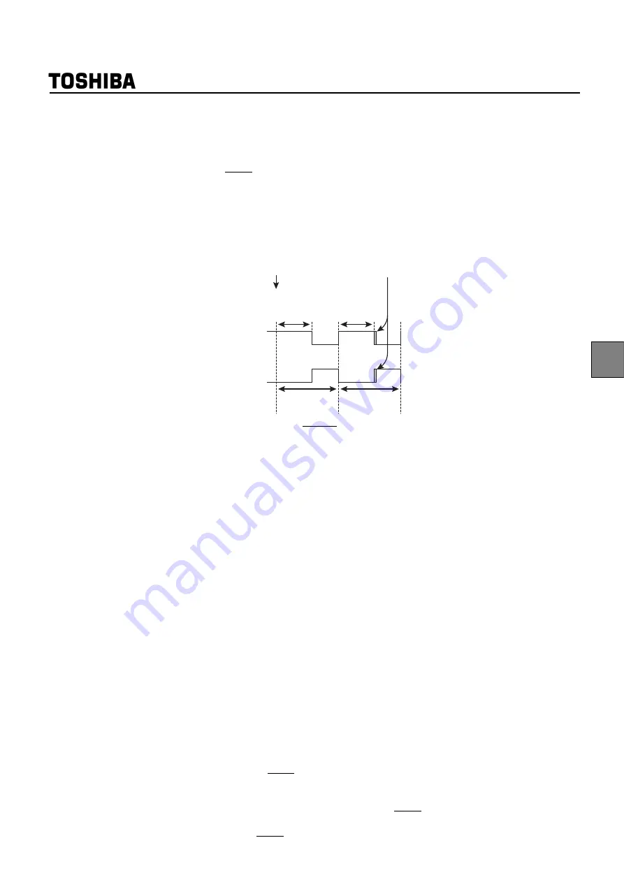
Figure 14-14
PWM1
Pin Output
14.4.7.3 Double buffer
The double buffer can be used for T01+00PWM by setting T01MOD<DBE1>. The double buffer is dis-
abled by setting T01MOD<DBE1> to "0" or enabled by setting T01MOD<DBE1> to "1".
• When the double buffer is enabled
When write instructions are executed on T00PWM and T01PWM in this order during the
timer operation, the set value is first stored in the double buffer, and T01+00PWM is not
updated immediately. T01+00PWM compares the previous set value with the up counter value.
When the 16
×
n-th overflow occurs, an INTT01 interrupt request is generated and the double
buffer set value is stored in T01+00PWM. Subsequently, the match detection is executed using
a new set value.
When a read instruction is executed on T01+00PWM (T00REG), the value in the double
buffer (the last set value) is read out, not the T01+00PWM value (the currently effective value).
When write instructions are executed on T00PWM and T01PWM in this order while the
timer is stopped, the set value is immediately stored in both the double buffer and
T01+00PWM.
• When the double buffer is disabled
When write instructions are executed on T00PWM and T01PWM in this order during the
timer operation, the set value is immediately stored in T01+00PWM. Subsequently, the match
detection is executed using a new set value. If the value set to T01+00PWM is smaller than the
up counter value, the
PWM1
pin is not reversed until the up counter overflows and a match
detection is executed using a new set value. If the value set to T01+00PWM is equal to the up
counter value, the match detection is executed immediately after data is written into
T01+00PWM. Therefore, the timing of changing the
PWM1
pin may not be an integral multiple
of the source clock. Similarly, if T01+00PWM is set during the additional pulse output, the tim-
ing of changing the
PWM1
pin may not be an integral multiple of the source clock. If these are
problems, enable the double buffer.
PWMDUTY
Timer start
Additional
pulse
(1 source clock)
(Duty pulse
width)
256 counts
(cycle width)
256 counts
(cycle width)
PWM1 pin output
(TFF0=“1”)
PWMDUTY
(Duty pulse
width)
PWM1 pin output
(TFF0=“0”)
Summary of Contents for TLCS-870/C1 Series
Page 1: ...8 Bit Microcontroller TLCS 870 C1 Series TMP89FM42 查询TMP89FM42供应商 捷多邦 专业PCB打样工厂 24小时加急出货 ...
Page 3: ...Revision History Date Revision 2007 10 25 1 First Release 2007 11 3 2 Contents Revised ...
Page 4: ......
Page 14: ......
Page 18: ...1 3 Block Diagram TMP89FM42 1 3 Block Diagram Figure 1 2 Block Diagram ...
Page 22: ...1 4 Pin Names and Functions TMP89FM42 ...
Page 60: ...2 CPU Core 2 5 Revision History TMP89FM42 ...
Page 76: ...3 Interrupt Control Circuit 3 8 Revision History TMP89FM42 ...
Page 86: ...4 External Interrupt control circuit 4 3 Function TMP89FM42 ...
Page 102: ...7 Voltage Detection Circuit 7 5 Revision History TMP89FM42 ...
Page 126: ...8 I O Ports 8 3 I O Port Registers TMP89FM42 Note 2 i 0 to 1 ...
Page 136: ...8 I O Ports 8 5 Revision History TMP89FM42 ...
Page 142: ...9 Special Function Registers 9 3 SFR3 0x0E40 to 0x0EFF TMP89FM42 ...
Page 146: ...10 Low Power Consumption Function for Peripherals TMP89FM42 ...
Page 149: ...TMP89FM42 11 3 Revision History Rev Description RA001 Deleted SLEEP2 description ...
Page 150: ...11 Divider Output DVO 11 3 Revision History TMP89FM42 ...
Page 220: ...15 Real Time Clock RTC 15 4 Real Time Clock Operation TMP89FM42 ...
Page 250: ...16 Asynchronous Serial Interface UART 16 15 Revision History TMP89FM42 ...
Page 302: ...18 Serial Bus Interface SBI 18 7 Revision History TMP89FM42 ...
Page 338: ...21 Flash Memory 21 4 Toggle Bit D6 TMP89FM42 ...
Page 384: ...22 Serial PROM Mode 22 15 Revision History TMP89FM42 ...
Page 388: ...24 Input Output Circuit 24 1 Control Pins TMP89FM42 ...
Page 404: ...25 Electrical Characteristics 25 11 Revision History TMP89FM42 ...
Page 406: ...26 Package Dimensions TMP89FM42 ...
Page 408: ......


