Verdin Carrier Board Design Guide
Preliminary
– Subject to Change
Toradex AG l Ebenaustrasse 10 l 6048 Horw l Switzerland l +41 41 500 48 00 l
l
Page | 46
between 1
Ω
and 10k
Ω
. A small pull-up resistor increases the power consumption while a large
resistor could lead to problems in the signal quality. The optimum size of the resistor depends on
the capacitive load on the I
2
C lines and the required bus speed.
2.9.1
I
2
C Signals
Verdin
Pin
Verdin
Signal Name
I/O
Type
Power
Rail
Description
14
I2C_1_SCL
I/O
OD
1.8V
General-purpose I
2
C interface
12
I2C_1_SDA
O
OD
1.8V
55
I2C_2_DSI_SCL
I/O
OD
1.8V
Dedicated I
2
C port for the MIPI DSI
53
I2C_2_DSI_SDA
O
OD
1.8V
59
I2C_3_HDMI_SCL
I/O
OD
1.8V
Dedicated I
2
C port for the HDMI port (DDC)
57
I2C_3_HDMI_SDA
O
OD
1.8V
95
I2C_4_CSI_SCL
I/O
OD
1.8V
Dedicated I
2
C port for the MIPI CSI
93
I2C_4_CSI_SDA
O
OD
1.8V
Table 21: I
2
C signals
2.9.2
Reference Schematics
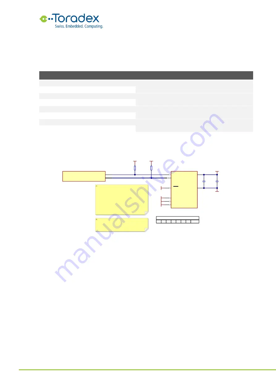
Figure 38: EEPROM Reference Schematic
2.9.3
Unused I
2
C Signal Termination
All unused I
2
C can be left unconnected if the according I
2
C port is switched off in software.
Otherwise, it is recommended to keep the pull-up resistors available. Unused I
2
C signals can be
configured as GPIO.
2.10
UART
There are four UART ports available in the Verdin module standard. UART_1 and UART_2 are
general purpose interfaces. The RX and TX signals of these interfaces are in the "Always
Compatible" section while the additional RTS/CTS signals for hardware flow control are in the
"Reserved" group.
UART_3 is in the "Always Compatible" section and is intended to be used for main OS debug log
output. It could be used for general purpose, but we recommend making this interface available
for debugging purposes. UART_4 is in the "Reserved" class. On modules with a real-time core, this
instance is intended to be used as the debug log output of the real-time operating system. The
interface may be used as general purpose UART.
E0
1
E1
2
E2
3
VSS
4
SDA
5
SCL
6
WC
7
VCC
8
IC30
M24C02-FMN6TP
I2C_1_SDA
12
I2C_1_SCL
14
X1M
2309409 -2
100nF
16V
C187
+V1.8_SW
GND
I2C_1_SCL
I2C_1_SDA
+V1.8_SW
+V1.8_SW
1uF
16V
C188
Slave address
1
1
0
E2
R/W
0
E1 E0
GND
1.8K
R263
1.8K
R264
E2,E1,E0 must be tied to VCC or VSS. When
not connected (left floating), these inputs are
read as low (0).
WC. Write operations are disabled to the
entire memory array when Write Control (WC)
is driven high. Write operations are enabled
when Write Control (WC) is either driven low
or left floating.
When Write Control (WC) is driven high,
device select and address bytes are
acknowledged, Data bytes are not
acknowledged.
GND
GND
GND


