background image

27 


Figure 22: TPS40100EVM-001 Layer 2 (X-Ray View from Top) 

Summary of Contents for TPS40100

Page 1: ... Load and low voltage bus converters Merchant Power Modules Networking Equipment Telecommunications Equipment DC Power Distributed Systems 2 2 FEATURES 10 8V 13 2V input range 3 3V fixed output 10 Adc Steady State Output Current Output margin up and down support Tracking voltage input to support simultaneous sequencing Power good indicator Frequency synchronization input Remote sensing scheme 380k...

Page 2: ...in up and down feature of the EVM provides the user with the ability to trim or margin the output of the converter up down by 3 or 5 EVM is equipped with convenient jumper settings to give the user the ability to trim the output voltage Please see section 5 3 5 in the test set up section of this users guide for more detailed test setup information 2 2 5 POWER GOOD J1 The EVM contains a power good ...

Page 3: ...S Output Voltage 3 22 3 30 3 39 V Output Voltage Regulation Line Regulation 10 8V VIN 13 2V IOUT 5A Load Regulation 0A IOUT 10A VIN 12V 1 1 Output Voltage Ripple VIN 13 2V IOUT 10A 25 mVpp Output Load Current 0 10 A Output Over Current 15 A SYSTEM CHARACTERISTICS Switching Frequency 350 380 410 kHz Full Load Efficiency VOUT 3 3V IOUT 10A V12V_IN 10 8V V12V_IN 12V V12V_IN 13 2V 93 9 93 5 93 4 Table...

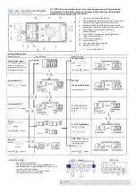
Page 4: ...4 4 SCHEMATIC Figure 1 TPS40100EVM 001 Power Stage Control Schematic ...

Page 5: ...5 Figure 2 TPS40100EVM 001 Margin Control Component values are for reference only ...

Page 6: ...ent response J2 to LOAD1 Remote Sense If remote sense is to be used ensure that J6 and J7 are in the remote sense enable position shunt pins 1 2 Load wires and sense wires should be kept less than 6 inches to ensure proper functionality The remote sense wires connecting J5 pins 1 and 4 and LOAD1 carry less than 1Adc The minimum recommended wire size is AWG 22 with the total length of less than 6 i...

Page 7: ... be worn 2 Prior to connecting the DC input source VIN it is advisable to limit the source current to 5 0A maximum Make sure VIN is initially set to 0V and connected as shown in Figure 4 3 Connect an ammeter between the positive output of the input supply and the positive input of the EVM J2 Pin 1 4 Connect voltmeter Voltmeter 1 to TP3 and TP4 as shown in Figure 2 1 These are the EVM input supply ...

Page 8: ...ote SenseJumper Disabled RemoteGNDSenseJumper Disabled 1 2 3 4 TP18 TP17 Metal Ground Barrel Probe Tip Tip and Barrel Vout ripple and transient measurement for TP17 and TP18 TP17 TP18 J8 J7 J6 1 2 3 1 2 3 Figure 4 TPS40100EVM 001 Recommended Test Set Up 5 2 3 START UP SHUT DOWN PROCEDURE 1 Increase VIN V1 from 0V to 12Vdc 2 Observe that Vout has risen to its nominal voltage 3 Vary LOAD1 from 0 10A...

Page 9: ...ut with R1 R3 5 3 2 Remote Sense Test Set Up In order for the remote sense feature of the TPS40100EVM 001 to function properly it is essential that the test setup be configured correctly Use the following steps to set up the remote sense 1 Ensure that the remote sense jumpers J7 J8 are shunted across pins 1 2 2 Connect load wires of a max length of 6 inches from pin 2 of J5 Vout to the positive te...

Page 10: ...oltagemonitoredattheoutput connector NOTE Thisw illread ahigher valueasloadcurrentincreases Voltagew illberegulatedtoset voltageattheLOAD Voltagemonitoredattheload Readingcanbetakenatthe load if desired NOTE Thisis thepointtow hichtheconverter w illberegulatingto 4 2 3 1 Figure 5 TPS40100EVM 001 Recommended Remote Test Set Up 5 3 3 Voltage Tracking Test Set Up The following procedure is for a sing...

Page 11: ...r TrackingEngageS2 TrackingEngageS2 Closed Dischargetrackingvoltagesignal Open Chargetrackingvoltagesignal LOAD1 3 3V 3A 3 3Vout TP13 TP14 J5 Voltmeter 2 Vout Scope JackTP 17 18 1MΩ DC 1V div 60mHzBW Remote SenseJumper Disabled RemoteGNDSenseJumper Disabled 1 2 3 4 TP3 Module toModule TP J8 J6 J7 Figure 6 TPS40100EVM 001 Single EVM Tracking Test Set Up ...

Page 12: ...12 Single unit tracking Charge Channel 1 3 3Vout Channel 4 Tracking In Vin 12V Iout 10A Figure 7 Single EVM tracking charging ramp ...

Page 13: ...sed shorting pins 2 3 position on the control EVMs 5 Connect oscilloscope probe to the TP17 and 18 of both modules and pin 1 of J3 of one of the modules Modules should have a common input voltage and return 6 Remote sense jumpers J6 7 should have pins 2 3 shunted Activating local output sensing 7 Apply an input voltage of 10 8V to 13 2V 8 Allow the SS voltage to reach 3 5V 9 Open the control EVM T...

Page 14: ...DSenseJumper Disabled 1 2 3 4 TP16 Moduleto Module TP J8 J6 J7 TP3 TP4 J2 TrackingEnable Jumper EnableS1 J3 4 1 2 3 ConnectorJ3 Pin 1Tracking In Pin2 3Gnd Pin4 EnableMonitor Tracking EngageS2 TrackingEngageS2 Closed Discharge trackingvoltagesignal Open Chargetracking voltagesignal LOAD1 1 8V 3A 3 3Vout TP13 TP14 J5 Voltmeter 2 Vout Scope JackTP 17 18 Remote SenseJumper Disabled RemoteGNDSenseJumpe...

Page 15: ... enable the device providing that the appropriate input voltage is present J3 pin 4 is an enable monitor pin providing a connection for user observation TP1 TP2 TP16 J2 TrackingEnable Jumper Margin Up 5 Margin Up 3 Margin Down 3 Margin Down 3 1 12 9 6 11 8 5 13 10 7 4 3 2 1 EnableS1 EnableSw itch logic Enable Open Disable Closed J3 1 5 1 4 4 1 2 3 ConnectorJ3 Pin 1Tracking In Pin2 3Gnd Pin4 Enable...

Page 16: ...16 Iout 10A Figure 11 Power on from enable ...

Page 17: ...est Set Up Example To margin the unit up 5 connect jumper across pins 2 and 3 of J4 TP1 TP2 TP16 J2 GND GND GNDGND TrackingEnable Jumper J4 MarginEnable Tomargintheunitshunt theassociatedpins Example Marginup5 shuntpins2and3 EnableSW1 TrackingLow SW2 Margin Up 5 Margin Up 3 Margin Down 3 Margin Down 5 1 15 12 9 6 14 11 8 5 13 10 7 4 3 2 1 2 3 Figure 12 TPS40100EVM 001 Margin Test Set Up Margin up ...

Page 18: ...nge from 0 4 5V dependent on the condition of the output A low on this pin dictates a power fault and a high 4 5V conveys power ok Pin 4 of J1 is the input for an external clock frequency To test set up a function generator to provide a square wave at a frequency of above 410 kHz and below 480 kHz Function generator should be set to provide a 0 to 5V square wave with a 50 duty cycle Once power is ...

Page 19: ...ingEngageS2 EnableSW1 SquareWave Freq 120 SWF 5Vpeak Function Generator POWER GOOD SYNC IN 1MΩ DC 1V div 60mHzBW TP9 LDRV J1 Pin1Pow erGood Pin2 3Gnd Pin 4 SYNC IN Voltmeter Figure 14 TPS40100EVM 001 Power Good and Synchronization Test Set Up Synchronization ...

Page 20: ... TYPICAL PERFORMANCE DATA CHARACTERISTIC CURVES Figure 16 through Figure 18 present typical performance curves for the TPS40100EVM 001 Since actual performance data can be affected by measurement techniques and environmental variables these curves are presented for reference and may differ from actual field measurements ...

Page 21: ...CY HPA089A Efficiency Line Load vs Efficiency 80 82 84 86 88 90 92 94 96 0 1 2 3 4 5 6 7 8 9 10 Load Current A Efficiency 10 8v 12 0v 13 2v Figure 16 TPS40100EVM 001 Efficiency V12V_IN 10 8 13 2V VOUT 3 3V IOUT 0 10A ...

Page 22: ...9A Load Regulation Vout vs Load Current 3 295 3 297 3 299 3 301 3 303 3 305 3 307 3 309 3 311 3 313 3 315 0 1 2 3 4 5 6 7 8 9 10 Load Current A Vout V 12 0v 10 8v 13 2v Figure 17 TPS40100EVM 001 Line Regulation IOUT 10A Vin 10 8 13 2V ...

Page 23: ...EMBLY DRAWINGS AND LAYOUT The following figures Figure 19 through 24 show the design of the TPS40100EVM 001 printed circuit board The EVM has been designed using a 4 layer 2oz copper clad circuit board 3 0 x 3 25 with most of the components on the top side to allow the user to easily view probe and evaluate the TPS40100 control IC in a practical application Moving components to both sides of the P...

Page 24: ...24 Figure 19 TPS40100EVM 001 Component Placement Viewed from Top ...

Page 25: ...25 Figure 20 TPS40100EVM 001 Silkscreen Viewed from Top ...

Page 26: ...26 Figure 21 TPS40100EVM 001 Top Copper Viewed from Top ...

Page 27: ...27 Figure 22 TPS40100EVM 001 Layer 2 X Ray View from Top ...

Page 28: ...28 Figure 23 TPS40100EVM 001 Layer 3 X Ray View from Top ...

Page 29: ...29 Figure 24 Bottom Copper X Ray View from Top 8 LIST OF MATERIALS Table 3 lists the EVM components as configured according to the schematic shown in Figure 1 and Figure 2 ...

Page 30: ...5750X7R1C226M TDK 1 C20 0 1uF Capacitor Ceramic 0 1 uF 6 3 V X5R 10 0805 C2012X5R0J226K TDK 1 C22 100uF Capacitor Ceramic 100 uF 6 3 V X5R 20 1812 Std Std 1 C24 1 0 uF Capacitor Ceramic 1 0 uF 50 V X7R 20 0603 Std Std 1 C25 1500pF Capacitor Ceramic 1500 pF 50 V X7R 10 0805 Std Std 1 C26 220uF Capacitor POSCAP 220 uF 10 V 12 milliohm 20 7343 D 10TPB220M Sanyo 2 C6 C13 068uF Capacitor Ceramic 0 068 ...

Page 31: ...20A 3 00 milliohms 0 512 x 0 551 inch PG0077 202 Pulse Engineering 1 Q1 HAT2168H Mosfet N Ch Vds 30V Rds 7 9 milliohms Id 30A LFPAK HAT2168H Hitachi 1 Q2 HAT2160H Mosfet N Ch Vds 20V Rds 2 6 milliohms Id 60A LFPAK HAT2160H Hitachi 4 Q3 Q4 Q5 Q6 2N7002 MOSFET N ch 60 V 115 mA 1 2 Ohms SOT23 2N7002DICT Vishay Liteon 1 R1 12 4k Resistor Chip 12 4kOhms 1 16 W 1 0603 Std Std 1 R10 42 2k Resistor Chip 4...

Page 32: ...3 Std Std 1 R6 1 62k Resistor Chip 1 62k Ohms 1 16 W 1 0603 Std Std 1 R7 110k Resistor Chip 110k Ohms 1 16 W 1 0603 Std Std 1 R8 15 0k Resistor Chip 15 0k Ohms 1 16 W 1 0603 Std Std 1 R9 127k Resistor Chip 127kOhms 1 16 W 1 0603 Std Std 2 S1 S2 Switch ON ON Mini Toggle Initial switch position closed shorting pins 1 2 0 28 x 0 18 G12AP NKK 5 TP1 TP2 TP4 TP12 TP14 5011 Test Point Black Thru Hole 0 1...

Page 33: ...24 TPS40100RGE TI 1 PCB 3 25 In x 3 0 In x 0 062 In EVM Any Notes 1 These assemblies are ESD sensitive ESD precautions shall be observed 2 These assemblies must be clean and free from flux and all contaminants Use of no clean flux is not acceptable 3 These assemblies must comply with workmanship standards IPC A 610 Class 2 4 Ref designators marked with an asterisk cannot be substituted All other c...

Page 34: ...Mouser Electronics Authorized Distributor Click to View Pricing Inventory Delivery Lifecycle Information Texas Instruments TPS40100EVM 001 ...

Reviews: